TFT array substrate and preparation method thereof and display device

A thin film transistor and array substrate technology, applied in the display field, can solve the problems of difficulty, poor copper etching ability, and high etching solution development cost, and achieve the effects of improving yield, blocking copper diffusion, and reducing costs.

Active Publication Date: 2014-03-19
BOE TECH GRP CO LTD
View PDF3 Cites 22 Cited by
  • Summary
  • Abstract
  • Description
  • Claims
  • Application Information

AI Technical Summary

Problems solved by technology

However, the patterned copper gate electrode needs to have a certain slope angle to prevent the fault of the gate insulating layer, which leads to the fact that the barrier layer cannot completely cover the upper surface of the copper film, and some copper is still exposed outside the protective layer at the boundary.
[0005] 2. The etching ability of copper is poor. It is very difficult to etch by wet or dry etching. The etching effect is not ideal, and the development cost of etching solution is relatively high.

Method used


Image

  • TFT array substrate and preparation method thereof and display device
  • TFT array substrate and preparation method thereof and display device
  • TFT array substrate and preparation method thereof and display device

Examples


preparation example Construction

[0064] The present invention also provides a method for preparing the thin film transistor array substrate provided by the above technical solution, comprising the following steps:

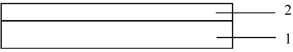
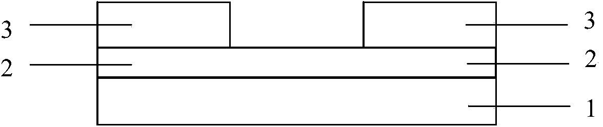
[0065] A first insulating layer 2 is formed on the substrate 1, and a first photoresist layer 3 is formed on the first insulating layer 2, and a gate recess is formed on the first insulating layer 2 formed with the first photoresist layer 3. a groove, the gate groove is surrounded by a first insulating layer;

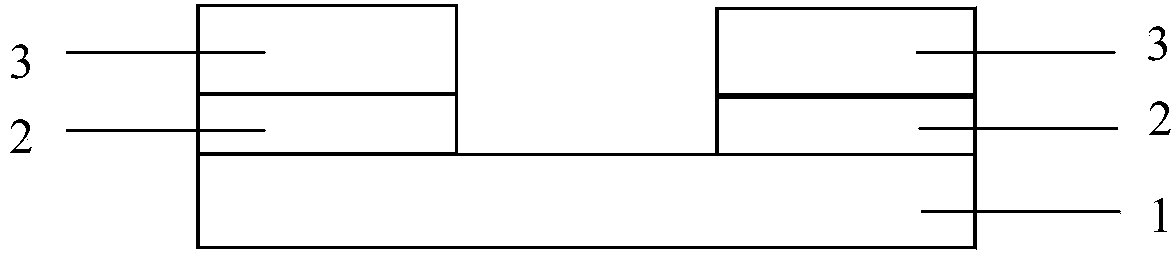
[0066] forming a gate layer on a substrate 1 having gate grooves;

[0067] The first photoresist layer 3 on the substrate on which the gate layer is formed and the gate layer above the first photoresist layer 3 are peeled off to form a gate 4 surrounded by the first insulating layer.


PUM


Abstract

The invention relates to the technical field of display and discloses a TFT (thin film transistor) array substrate and a preparation method thereof and a display device which includes the TFT array substrate. A grid is formed in a grid groove of a first insulating layer so that the grid is surrounded by the first insulating layer. The graphic grid does not have any gradient. The first insulating layer separates the grid from the outside so that fault of the grid insulating layer can be prevented and thus copper diffusion in the TFT array substrate can be blocked effectively. Furthermore, the upper surface and / or lower surface of a composite copper metal or a composite thin-film layer including the copper metal are / is completely covered with a metal block layer so that a role of blocking of the copper diffusion is well played. At the same time, more importantly, etching of the copper is not needed so that cost is reduced and yield is improved.

Description

technical field [0001] The invention relates to the field of display technology, in particular to a thin film transistor array substrate, a display device thereof, and a display device. Background technique [0002] At present, relatively stable metals such as Ta, Mo, Cr or alloy materials such as AlNd are generally used to make the scan lines and data lines on the array substrate of the thin film transistor (TFT for short) of the display. With the development of display technology, the size of the display continues to increase and the resolution continues to increase. Products such as large TVs or high-resolution monitors also require the RC delay (ie, resistance / capacitance delay) of scan lines and data lines to be small. It is required to use materials with lower resistivity for scanning lines and data lines. [0003] Among metal materials, copper has lower resistivity and is the preferred material that can replace existing aluminum and aluminum alloy materials and reduc...

Claims


Application Information

Patent Timeline
Patent Type & Authority Applications(China)
IPC IPC(8): H01L21/84H01L21/28H01L27/12H01L29/423
CPCH01L21/76841H01L23/5386H01L27/124H01L27/1259H01L29/4236H01L29/40114H01L29/4908H01L29/66969H01L29/7869H01L21/28008H01L21/283H01L21/3081H01L29/41733H01L29/42384H01L29/66742H01L29/786
Inventor 刘凤娟王美丽张立闫梁臣
Owner BOE TECH GRP CO LTD
Why Eureka
Try Eureka