Formation method of semiconductor structure

A semiconductor and dry etching technology, which is applied in semiconductor devices, semiconductor/solid-state device manufacturing, electrical components, etc., can solve problems such as leakage current, threshold voltage drift, and influence on integrated circuit performance, and achieve the effect of increasing the etching rate

Active Publication Date: 2016-02-17
SEMICON MFG INT (SHANGHAI) CORP
View PDF4 Cites 0 Cited by
  • Summary
  • Abstract
  • Description
  • Claims
  • Application Information

AI Technical Summary

Problems solved by technology

[0005] However, transistors produced by existing technologies often have problems such as leakage current and threshold voltage drift, which affect the performance of integrated circuits

Method used


Image

  • Formation method of semiconductor structure
  • Formation method of semiconductor structure
  • Formation method of semiconductor structure

Examples


Embodiment Construction

[0032] As mentioned in the background art, there are problems such as leakage current and unstable threshold voltage of fin field effect transistors at present, which affect the performance of transistors and integrated circuits.

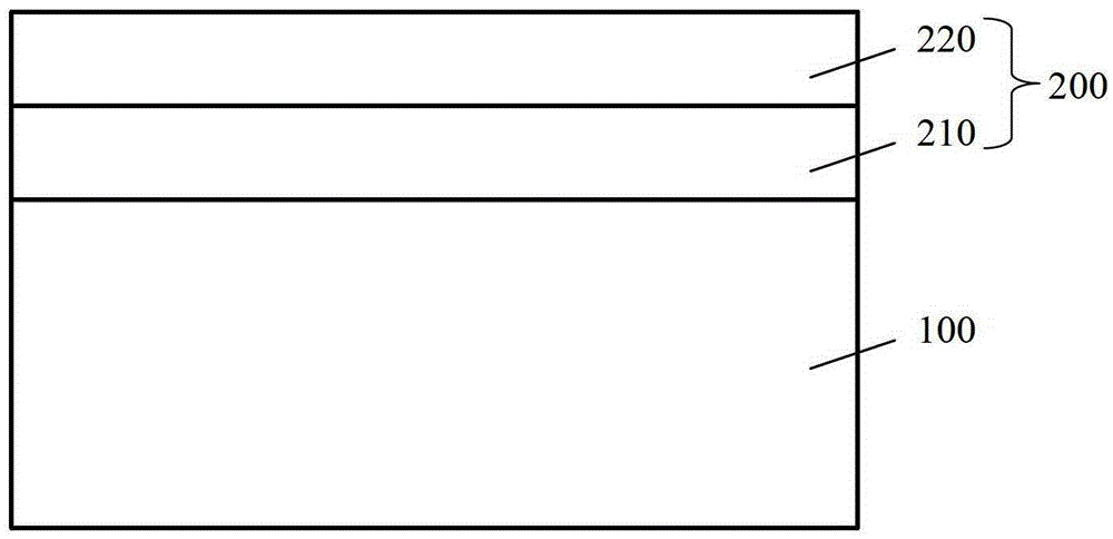
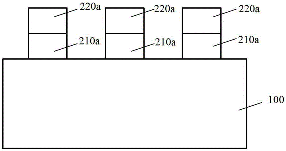
[0033] After research, it is found that in the FinFET, the quality of the interface between the gate structure and the fin has a great influence on the performance of the FinFET. The study found that compared with the Si(110) surface, the Si(551) surface is easier to arrange atoms, has fewer surface defects, and has a higher current driving capability. The Si (551) crystal plane is an inclined plane, and the fins with inclined sidewalls are more conducive to the deposition of the gate structure and improve the interface quality. However, in the prior art, most of the fins with inclined sidewalls have complicated process and need to etch the fins multiple times, which is easy to cause damage to the sidewalls of the fins.

[0034] In order to solve t...


PUM


Abstract

The invention provides a method for forming a semiconductor structure. The method comprises the following steps: providing a semiconductor substrate; forming a first hard mask structure on the surface of the semiconductor substrate, wherein the first hard mask structure has a bottom surface in contact with the semiconductor substrate, and the bottom surface is positioned within the projection of the first hard mask structure on the surface of the semiconductor substrate; taking the first hard mask structure as mask, etching the semiconductor substrate to form a fin part whose side walls are inclined. The method for forming a semiconductor structure also comprises the following steps: forming a gate structure on the surface of the fin part, the gate structure going across the top surface and the side wall of the fin part; forming a source and a drain at two ends of the fin part, wherein the source and the drain is positioned on two sides of the gate structure. The method for forming a semiconductor structure can form a fin-type field-effect transistor in which the side walls of the fin part are inclined and the inclined side walls of the fin part have a smooth surface, as a result, the performance of the fin-type field-effect transistor is improved.

Description

technical field [0001] The invention relates to the technical field of semiconductors, in particular to a method for forming a semiconductor structure. Background technique [0002] With the continuous development of semiconductor process technology, process nodes are gradually reduced, and gate-last (gate-last) process has been widely used to obtain an ideal threshold voltage and improve device performance. But when the feature size (CD, Critical Dimension) of the device is further reduced, even the field effect transistor manufactured by the gate-last process can no longer meet the demand for device performance, and the multi-gate device has received extensive attention. [0003] Fin field effect transistor (FinFET) is a common multi-gate device, figure 1 A three-dimensional schematic diagram of a fin and a gate structure of a fin field effect transistor in the prior art is shown. Such as figure 1 As shown, it includes: a semiconductor substrate 10, a protruding fin 14 ...

Claims


Application Information

Patent Timeline
Patent Type & Authority Patents(China)
IPC IPC(8): H01L21/336
CPCH01L29/7853
Inventor 孟晓莹隋运奇
Owner SEMICON MFG INT (SHANGHAI) CORP
Why Eureka
Try Eureka