
Method for manufacturing semiconductor device

A manufacturing method, semiconductor technology, applied in the direction of semiconductor/solid-state device manufacturing, semiconductor devices, electric solid-state devices, etc., can solve problems affecting surface flatness, side wall damage, large porosity, etc., and achieve the effect of ensuring surface flatness

Active Publication Date: 2014-03-26
SEMICON MFG INT (SHANGHAI) CORP
View PDF5 Cites 4 Cited by
  • Summary
  • Abstract
  • Description
  • Claims
  • Application Information

AI Technical Summary

Problems solved by technology

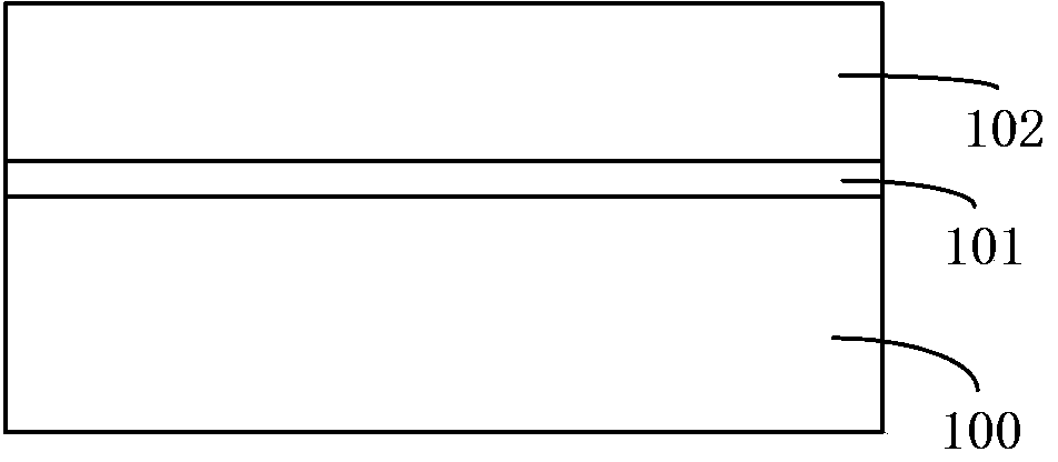
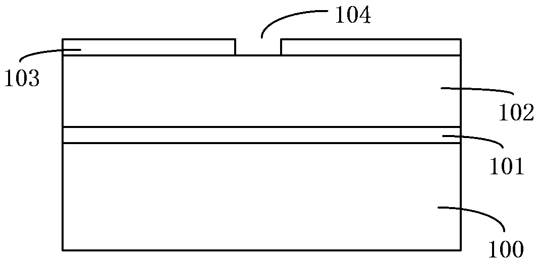
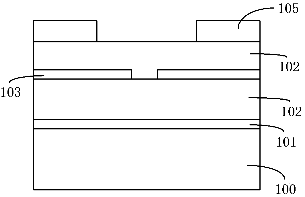
[0004] In order to realize the final communication with the active device layer, the etch stop layer 101 under the through hole 107 needs to be removed. The carrier gas is usually nitrogen (N 2 ), the exposed copper interconnect metal in the active device layer reacts with nitrogen to form a substance (Cu x N y ), this substance is difficult to remove; at the same time, since the material constituting the interlayer dielectric layer 102 has a large porosity, the main component is CF 4 The plasma etching gas also seriously damages the sidewall of the interlayer dielectric layer 102. Therefore, the above phenomenon will affect the surface flatness of the sidewall and bottom of the through hole 107, which is not conducive to the subsequent copper barrier. layer formation, which eventually leads to the intensification of the diffusion of Cu metal

Method used


Image

  • Method for manufacturing semiconductor device
  • Method for manufacturing semiconductor device
  • Method for manufacturing semiconductor device

Examples


Embodiment approach 1

[0039] CF-based 4 and N 2 The etching gas is used to perform the plasma etching; then, a post-etch process is performed to remove the etching residues and impurities formed in the trench 206 and the through hole 207; finally, using CF-based 4 , CO 2 and CO etching gases again perform the plasma etching, wherein the CF 4 The flow rate is 50-500sccm, the N 2 The flow rate is 10-500sccm, the CO 2 The flow rate of CO is 10-500 sccm, the flow rate of CO is 10-500 sccm, the pressure of the two plasma etching is 10-100 mTorr, the power is 100-500 W, and the processing time is 10-60 s.

Embodiment approach 2

[0041] First perform a post-etching process to remove the etching residues and impurities formed in the trench 206 and the through hole 207; then, using CF 4 , CO 2 and CO etching gas to perform the plasma etching, wherein the CF 4 The flow rate is 50-500sccm, the CO 2 The flow rate of the CO is 10-500 sccm, the CO flow rate is 10-500 sccm, the plasma etching pressure is 10-100 mTorr, the power is 100-500 W, and the processing time is 10-60 s.

[0042] So far, all the process steps implemented by the method according to the exemplary embodiment of the present invention are completed. Next, a copper metal diffusion barrier layer and a copper metal layer are sequentially formed in the trench 206 and the through hole 207 . According to the present invention, when etching the etch stop layer under the via hole, the damage to the interlayer dielectric layer is small, and no substance that is difficult to remove by the post-etching process is formed at the bottom of the via hole. ...


PUM


Abstract

The invention provides a method for manufacturing a semiconductor device. The method comprises the following steps: providing a semiconductor substrate; sequentially forming an etching stopping layer and an interlayer dielectric layer on the semiconductor substrate; forming a groove and a through hole for filling interconnected metal; removing the etching stopping layer below the through holes by using a plasma etching process, wherein the removing process comprises the following steps: firstly, performing post-etching treatment process so as to remove residual etching substances and impurities formed in the groove and the through hole, and secondly performing plasma etching by using an etching gas based on CF4, CO2 and CO. According to the method, when the etching stopping layer below the through hole is etched, the damage to the interlayer dielectric layer is small, and moreover substances which are hard to be removed after the etching are not formed at the bottom of the through hole, so that the surface flatness of the side wall and the bottom of the through hole is ensured.

Description

technical field [0001] The invention relates to a semiconductor manufacturing process, in particular to a method for removing an etching stop layer under the through holes after forming trenches and through holes for filling interconnection metal. Background technique [0002] When the process node of the semiconductor manufacturing process reaches below 28nm, the interlayer dielectric layer used when forming the interconnection metal layer of the semiconductor device is usually composed of a material with an ultra-low dielectric constant in order to reduce the RC delay of the semiconductor device. [0003] Semiconductor devices generally have multiple layers of interconnect metal, and the process of forming trenches and vias for filling the interconnect metal includes the following steps: first, as Figure 1A As shown, a semiconductor substrate 100 is provided, and an active device layer is formed on the semiconductor substrate 100. For simplicity, only the semiconductor sub...

Claims


Application Information

Patent Timeline
IPC IPC(8): H01L21/768
CPCH01L21/31116H01L21/76805H01L2221/1005
Inventor 张海洋胡敏达
Owner SEMICON MFG INT (SHANGHAI) CORP
Learn More