

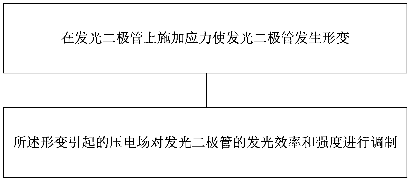
Light-emitting diode and modulation method for luminous efficiency and intensity of light-emitting diode
A technology of light-emitting diodes and luminous efficiency, which is applied in the direction of electrical components, circuits, semiconductor devices, etc., can solve the problems of low quantum efficiency and light extraction efficiency, and achieve the effects of increasing internal quantum efficiency, reducing light extraction loss, and increasing light extraction efficiency
- Summary
- Abstract
- Description
- Claims
- Application Information
AI Technical Summary
Problems solved by technology
Method used
Image

Examples
Embodiment 1
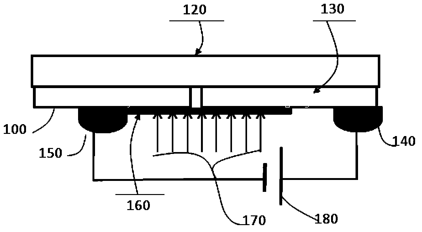
[0046] In the modulation method of light-emitting diode luminous efficiency and intensity in this embodiment, the light-emitting diode is composed of a semiconductor thin film and piezoelectric micro-nano wires on the semiconductor thin film, see figure 2 , the semiconductor film 130 and the conductive glass 100 are arranged on the substrate 120 apart, the thickness of the conductive glass 100 is basically the same as that of the semiconductor film 120, a groove is formed on the semiconductor film 130 and the conductive glass 100, and the piezoelectric micro-nano wire 160 is parallel to the semiconductor film and Across the groove, that is, one end of the piezoelectric micro-nano wire 160 is fixed on the semiconductor film 130 , and the other end is fixed on the conductive glass 100 , and the piezoelectric micro-nano wire 160 and the semiconductor film 110 form a light emitting diode. The electrode 150 at one end of the piezoelectric micro-nano wire 160 fixed on the conductive...
Embodiment 2
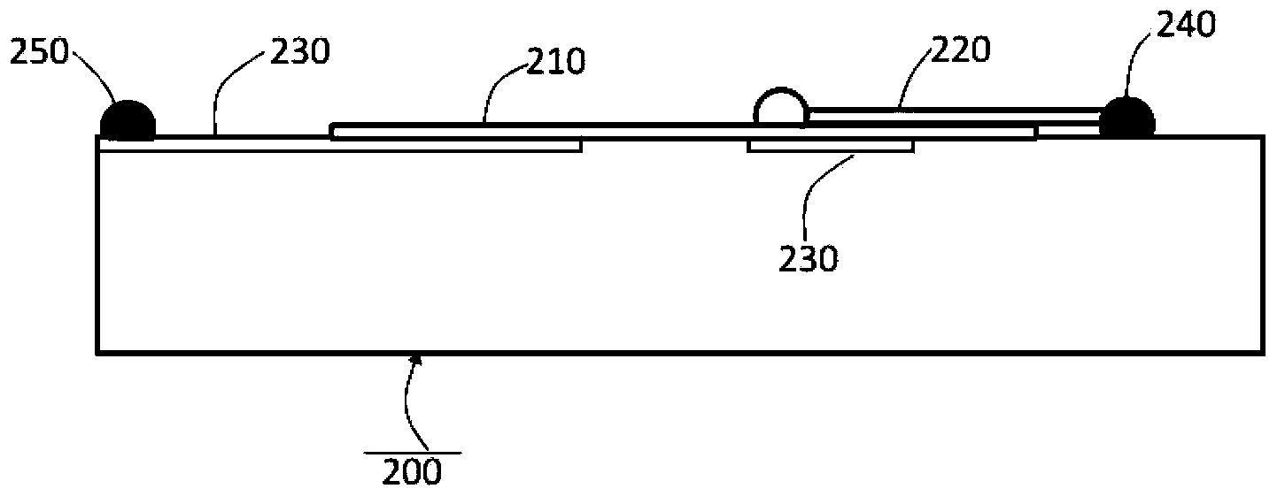
[0052] In the modulation method of light-emitting diode luminous efficiency and intensity in this embodiment, the light-emitting diode is composed of semiconductor thin film and piezoelectric micro-nano wire, see Figure 3a , prepare two metal or transparent conductive films 230 on the plastic material substrate 200, and form a groove between the two metal or transparent conductive films 230, and place semiconductor piezoelectric micro-nano wires 210 with piezoelectric properties on the substrate On the bottom, the piezoelectric micro-nanowire 210 is parallel to the metal or transparent conductive film 230 and straddles the trench, that is, the two ends of the piezoelectric micro-nanowire 230 are respectively fixed on the metal or transparent conductive film 230, and the semiconductor A polymer semiconductor or an inorganic semiconductor film 220 and a semiconductor micro-nano wire 210 are arranged on the piezoelectric micro-nano wire 210 to form a PN junction, and an anode ele...
Embodiment 3
[0058] In the modulation method of light-emitting diode luminous efficiency and intensity in this embodiment, the light-emitting diode is composed of a semiconductor thin film and piezoelectric micro-nano wires on the semiconductor thin film, see Figure 4 , the semiconductor film 310 is located on the substrate 300, the piezoelectric micro-nano wire 320 is substantially perpendicular to the semiconductor film 310, the piezoelectric micro-nano wire 320 and the semiconductor film 310 form a light-emitting diode, the semiconductor film 310 includes a bottom electrode 330, and the piezoelectric micro-nano wire 320 forms a light emitting diode. The nanowire 320 includes a top electrode 340 thereon. A power supply is connected between the bottom electrode 330 and the top electrode 340 of the light-emitting diode to drive the light-emitting diode to emit light; the stress F1 along the micro-nano wire 320 is applied to the top of the piezoelectric micro-nano wire 320, so that the micr...
PUM
| Property | Measurement | Unit |
|---|---|---|
| Diameter | aaaaa | aaaaa |
Abstract
Description
Claims
Application Information