Strong-field negative pulse Gunn diode and preparation method thereof

A Gunn diode and negative pulse technology, applied in the microwave field, can solve the problem of low output efficiency of the Gunn diode

Active Publication Date: 2014-03-26
无锡炬脉电源科技有限公司
View PDF5 Cites 0 Cited by
  • Summary
  • Abstract
  • Description
  • Claims
  • Application Information

AI Technical Summary

Problems solved by technology

[0004] The object of the present invention is a strong-field negative-pulse Gunn diode, which utilizes an appropriate device structure to realize that the strong-field negative-pulse Gunn diode works in the reverse Gunn...

Method used


Image

  • Strong-field negative pulse Gunn diode and preparation method thereof
  • Strong-field negative pulse Gunn diode and preparation method thereof
  • Strong-field negative pulse Gunn diode and preparation method thereof

Examples


Embodiment Construction

[0028] The present invention will be described in detail below in conjunction with the accompanying drawings and specific embodiments.

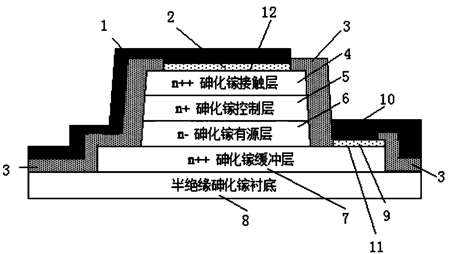
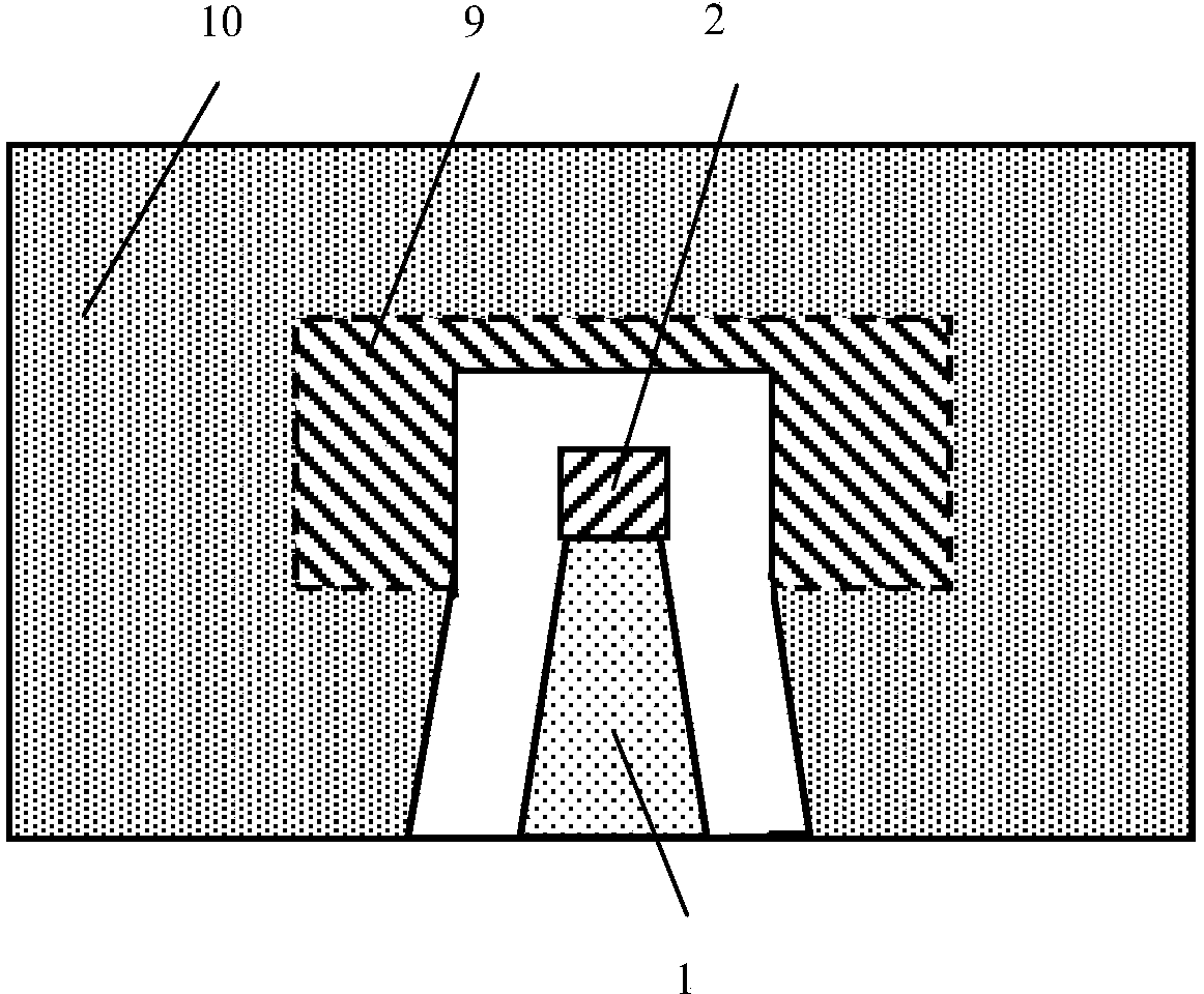
[0029] The present invention provides a strong-field negative pulse Gunn diode, which includes an epitaxial wafer, and the epitaxial wafer includes a semi-insulating gallium arsenide substrate 8, an n++ gallium arsenide buffer layer 7, an n-arsenide GaAs active layer 6, n+GaAs control layer 5 and n++GaAs contact layer 4, n++GaAs buffer layer 7 has an anode ohmic contact layer 9 on its upper surface, and an anode ohmic contact layer 9 has an anode on its upper surface Lead 10, the upper surface of the n++GaAs contact layer 4 is provided with a cathode ohmic contact layer 2, the upper surface of the cathode ohmic contact layer 2 is provided with a cathode lead 1, and the rest of the outer layer of the epitaxial wafer except the semi-insulating GaAs substrate 8 is provided There are Si 3 N 4 The passivation layer 3, wherein the n++ gallium ars...


PUM

PropertyMeasurementUnit
Doping concentrationaaaaaaaaaa

Abstract

The invention discloses a strong-field negative pulse Gunn diode which comprises an epitaxial wafer. The epitaxial wafer comprises a semi-insulating gallium arsenide substrate, an n++ gallium arsenide buffering layer, an n- gallium arsenide active layer, an n+ gallium arsenide control layer and an n++ gallium arsenide contact layer which are sequentially arranged from bottom to top, and the n- gallium arsenide active layer is 5-10 micrometers in length and 5x10¹⁵-8x1015cm-3 in doping concentration. The invention further discloses a preparation method of the strong-field negative pulse Gunn diode. A proper device structure is utilized to enable the Gunn diode to work in a reverse Gunn dipole domain mode, output power and efficiency of existing Gunn diodes can be improved by many times, and the problem that the existing Gunn diodes are low in output efficiency is solved.

Description

technical field [0001] The invention belongs to the field of microwave technology, and in particular relates to a strong field negative pulse Gunn diode, and also relates to a preparation method of the strong field negative pulse Gunn diode. Background technique [0002] The Gunn effect is an effect discovered by J.B. Gunn in 1963. When a certain constant DC voltage is applied to the contact electrode on the opposite side of a small piece of N-type gallium arsenide, microwave oscillation is generated. When a good ohmic contact electrode is made at the two ends of the N-type gallium arsenide sheet, and a DC voltage is applied to make the generated electric field exceed 3kV / cm, due to the negative differential mobility characteristic of gallium arsenide, current oscillation will occur, and its Frequency up to 10 9 Hz, this is the Gunn diode. This phenomenon of generating a high-frequency current in a semiconductor body is called the Gunn effect. [0003] Gunn diodes have v...

Claims


Application Information

Patent Timeline
IPC IPC(8): H01L47/02H01L47/00
Inventor 屈光辉
Owner 无锡炬脉电源科技有限公司
Why Eureka
Try Eureka