Gold-plated circuit board manufacturing method

A production method and circuit board technology, which is applied in the fields of printed circuit manufacturing, printed circuit, electrical components, etc., can solve problems such as burrs on gold-plated boards, achieve the effect of solving burrs and improving the pass rate

Active Publication Date: 2014-03-26
GUANGZHOU FASTPRINT CIRCUIT TECH +2
View PDF8 Cites 18 Cited by
  • Summary
  • Abstract
  • Description
  • Claims
  • Application Information

AI Technical Summary

Problems solved by technology

[0005] Based on this, the purpose of the present invention is to overcome the defects of the prior art and provide a method for manufacturing a gold-plated circuit board. Using this method, the problem of burrs on the gold-plated board can be solved without manual trimming, and the process is simple and easy to control. Greatly save labor costs and improve production efficiency

Method used


Image

  • Gold-plated circuit board manufacturing method
  • Gold-plated circuit board manufacturing method
  • Gold-plated circuit board manufacturing method

Examples


Embodiment 1

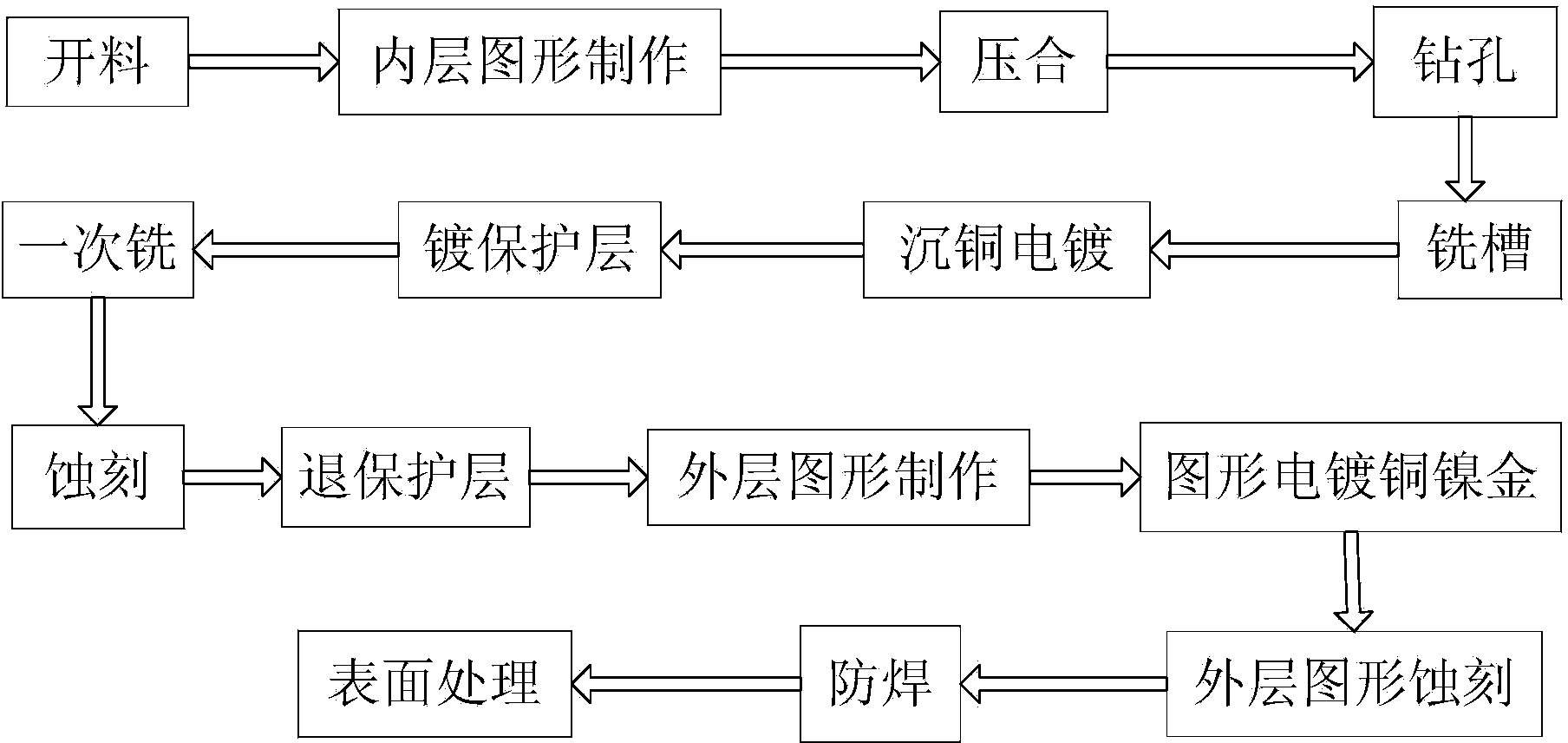
[0036] A method for making a gold-plated circuit board, such as figure 2 As shown, including material cutting, inner layer graphic production, pressing, drilling, milling, copper plating, protective layer plating, one-time milling, etching, protective layer removal, outer layer graphic production, graphic electroplating copper nickel gold, outer layer Layer graphic etching, solder mask, surface treatment process; among them:

[0037] Cutting, inner layer graphic making, pressing and drilling processes are handled according to the conventional process.

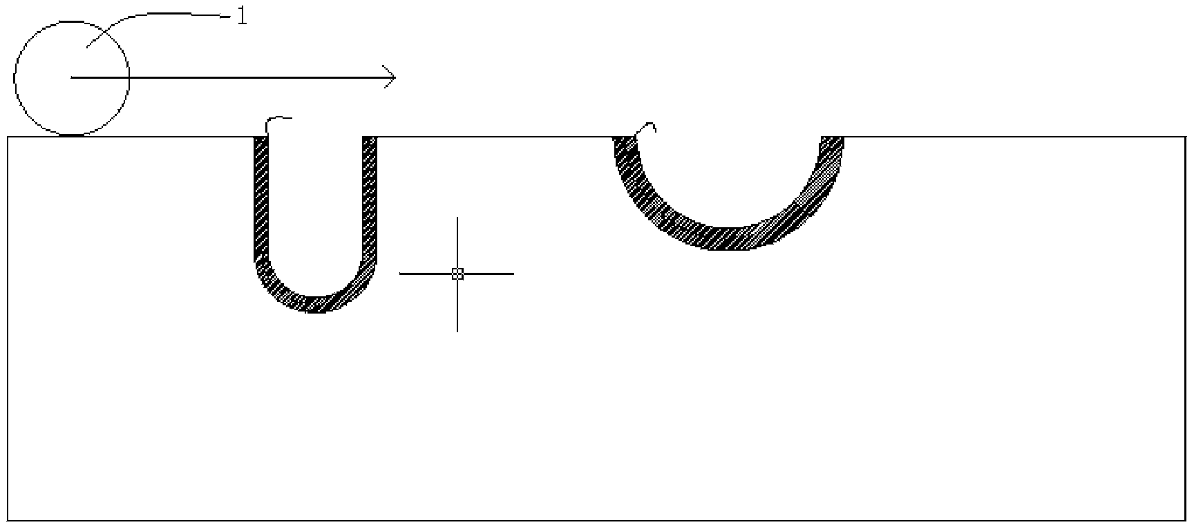
[0038] In the slot milling process, the side wall of the metallized area is processed in the way of slot milling 2, such as image 3 shown.

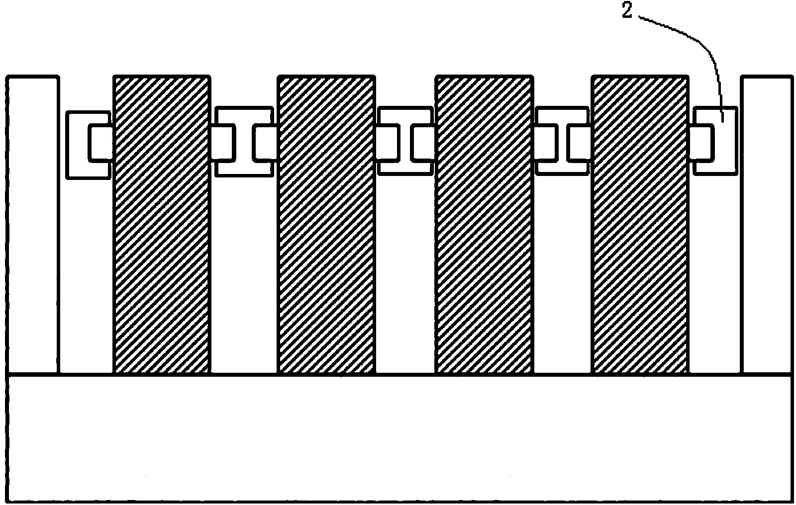
[0039] In the copper plating process, such as Figure 4 As shown, the milled slots are metallized by sinking copper, the electroplating process controls the current density to 8ASF, and the time is 25min, so that the copper thickness reaches 6μm.

[0040] In the step of plating the p...

Embodiment 2

[0048] The gold-plated circuit board manufacturing method of the present embodiment is basically the same as the manufacturing method in embodiment 1, the difference is:

[0049] In the copper immersion electroplating process, the milled slots are metallized by immersion copper. During the electroplating process, the current density is controlled at 15ASF, and the time is 60min, so that the copper thickness reaches 12μm.

[0050] In the step of plating the protective layer, the protective layer is a tin layer, and the thickness of the tin layer is 10 μm.

[0051] In the outer pattern making process, when the dry film is exposed, the exposed area of ​​the dry film is extended 5 mil into the groove.

[0052] In the graphic electroplating copper-nickel-gold process, copper plating and nickel plating are processed according to conventional processes. The conditions for gold plating are to control the current density to 3ASF for 120 seconds, so that the thickness of the gold layer re...

Embodiment 3

[0054] The gold-plated circuit board manufacturing method of the present embodiment is basically the same as the manufacturing method in embodiment 1, the difference is:

[0055] In the copper immersion electroplating process, the milled slots are metallized by immersion copper. During the electroplating process, the current density is controlled at 10ASF, and the time is 40min, so that the copper thickness reaches 9μm.

[0056] In the step of plating the protective layer, the protective layer is a tin layer, and the thickness of the tin layer is 7 μm.

[0057] In the process of making the outer pattern, when the dry film is exposed, the exposed area of ​​the dry film is extended 3mil into the groove.

[0058] In the graphic copper-nickel-gold plating process, copper plating and nickel plating are processed according to conventional processes. The conditions for gold plating are to control the current density to 2ASF for 90 seconds, so that the thickness of the gold layer reac...


PUM

PropertyMeasurementUnit
thicknessaaaaaaaaaa
thicknessaaaaaaaaaa
thicknessaaaaaaaaaa

Abstract

The invention discloses a gold-plated circuit board manufacturing method, and belongs to the technical field of the printed circuit board. The manufacturing method includes: cutting material, making an inner layer image, pressing, drilling, milling groove, precipitating copper electroplating, plating a protective layer, an one-time milling, etching, removing the protective layer, making an outer layer image, plating a copper nickel alloy for the image, etching of the outer layer image, a solder mask process, and a surface processing process. The manufacturing method can be used to solve the problem of the gold-plated burr, the artificial trimming is not needed, the simple process and easy control are realized, the labor cost is greatly saved, and the production efficiency is improved.

Description

technical field [0001] The invention relates to a process method of a printed circuit board, in particular to a method for manufacturing a gold-plated circuit board. Background technique [0002] With the continuous development of electronic products in the direction of multi-functionality, miniaturization, light weight and high performance, the requirements for miniaturization and high density of printed circuit boards are also increasing, and its products are also changing from traditional printed circuit boards to high-density Build-up printed board development. The key to the production of high-density laminated printed boards is the realization of ultra-high density and high reliability. Gold has good electrical conductivity, chemical stability and solderability. The gold plating layer is flat, bright, and has high corrosion resistance. Meet the high reliability requirements of high-density laminated printed boards, so its application range is expanding, such as photov...

Claims


Application Information

Patent Timeline
Patent Type & Authority Applications(China)
IPC IPC(8): H05K3/00
Inventor 陈曦刘攀曾志军
Owner GUANGZHOU FASTPRINT CIRCUIT TECH
Why Eureka
Try Eureka