Light-emitting diode and preparation method of buffer layer thereof

A technology for light-emitting diodes and buffer layers, which can be used in coatings, metal material coating processes, semiconductor/solid-state device manufacturing, etc., and can solve problems such as poor lattice matching.

Inactive Publication Date: 2014-04-02
江苏汉莱科技有限公司
View PDF4 Cites 6 Cited by
  • Summary
  • Abstract
  • Description
  • Claims
  • Application Information

AI Technical Summary

Problems solved by technology

[0004] In order to solve the problem of poor lattice matching between GaN-based and sapphire substrates and reduce the defect density, the inventors of the present invention, based on the existing technology, have conducted countless improvement tests on the buffer layer and found that when the epitaxy During epitaxy, the buffer layer is In x Ga 1-x The N structure replaces the

Method used


Image

  • Light-emitting diode and preparation method of buffer layer thereof
  • Light-emitting diode and preparation method of buffer layer thereof
  • Light-emitting diode and preparation method of buffer layer thereof

Examples


Embodiment 1

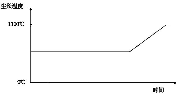
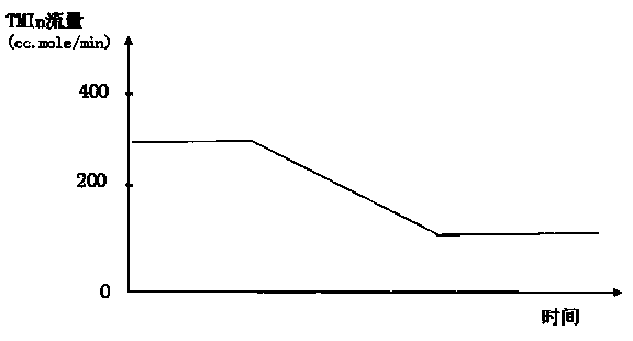
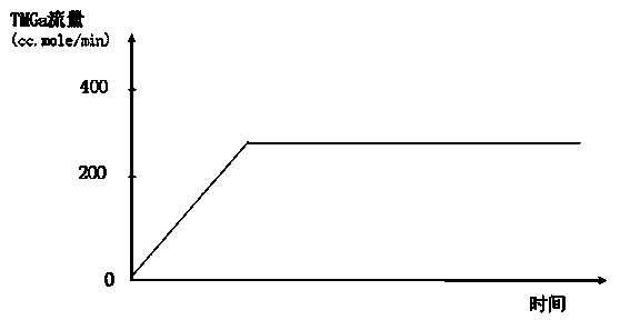
[0020] Grow Indium with a gradient of indium and gallium composition with a thickness of 400? on a sapphire substrate x Ga 1-x N buffer layer, before epitaxial growth, adjust the temperature to 550℃, pressure to 400torr, use nitrogen as the carrier gas, ammonia as the reaction gas, adjust the TMIn flow rate to 300cc.mole / min, and maintain the reaction conditions such as reaction temperature and pressure No change, control the flow rate of TMIn unchanged, start to pass into TMGa, and its flow rate will increase from 0cc.mole / min at a uniform rate. When the buffer layer grows to 1 / 4 of the total thickness of the buffer layer, the flow rate of TMGa reaches 300 cc.mole / min, the flow rate of TMIn begins to decrease at a uniform rate. When the buffer layer grows to 3 / 4 of its total thickness, the flow rate of TMIn decreases to 1 / 4 of the original flow rate. During the process, the flow rate of TMGa remains at 300 cc.mole / min. To maintain the flow rate of TMIn and TMGa at this time, i...

Embodiment 2

[0022] Growing on a sapphire substrate with a thickness of 250? Indium and gallium composition gradient change In x Ga 1-x N buffer layer, before epitaxial growth, adjust the temperature to 580℃, pressure to 350torr, use nitrogen as the carrier gas, ammonia as the reaction gas, adjust the TMIn flow rate to 310cc.mole / min, and maintain the reaction conditions such as reaction temperature and pressure No change, control the flow rate of TMIn unchanged, start to pass TMGa, its flow rate increases from 0cc.mole / min at a uniform rate, when the buffer layer grows to 1 / 4 of the total thickness of the buffer layer, the flow rate of TMGa reaches 295 cc.mole / min. At this time, the flow rate of TMIn decreases at a uniform rate. When the buffer layer grows to 3 / 4 of its total thickness, the flow rate of TMIn drops to 1 / 4 of the original flow rate. During the process, the flow rate of TMGa remains at 295 cc.mole / min. Maintain the flow rate of TMIn and TMGa at this time. During the last 1 / 4 ...


PUM


Abstract

The invention discloses a light-emitting diode and a preparation method of a buffer layer thereof. The light-emitting diode comprises a sapphire substrate, as well as a buffer layer, an N-type semiconductor layer, an active light-emitting layer and a P-type semiconductor layer which are sequentially formed on the sapphire substrate, wherein the buffer layer is made of INxGa1-xN; and in the growing process of the whole epitaxial buffer layer, the In content and the Ga content of the buffer layer are changed in gradient, and x constantly changes from 1 at the beginning to 0 at the end of the growth of the buffer layer, that is, the In amount in the buffer layer constantly descends and the Ga amount in the buffer layer constantly ascends.

Description

technical field [0001] The invention belongs to the field of light-emitting diode elements, and relates to a light-emitting diode, which improves the buffer layer structure and a preparation method of the buffer layer. Background technique [0002] With the continuous improvement of global environmental protection, energy saving and safety awareness in recent years, various energy saving and environmental protection products have been widely concerned, among which the promotion and application of light emitting diodes (LEDs) has attracted much attention. A light-emitting diode is a light-emitting device that converts electrical energy into light energy, and is mainly used in the fields of lighting, display, indication, and decoration. With the increasing awareness of energy saving and environmental protection around the world, light-emitting diodes have been widely used in recent years because of their good performance of "saving 80% of energy than energy-saving lamps". Many...

Claims


Application Information

Patent Timeline
IPC IPC(8): H01L33/12H01L33/32C23C16/455C23C16/34
CPCH01L33/12C23C16/303C23C16/455H01L21/0242H01L21/02458H01L21/0262
Inventor 林桂荣庄文荣孙明颜建锋敖辉
Owner 江苏汉莱科技有限公司
Why Eureka
Try Eureka