High-power semiconductor laser unit of low thermal stress structure

A semiconductor and laser technology, applied in the field of low-stress semiconductor lasers, can solve the problems of low thermal conductivity of semiconductor lasers, reduce the reliability of semiconductor lasers, and low thermal conductivity, and achieve the effects of high reliability, long life and narrow spectrum.

Active Publication Date: 2014-04-09
FOCUSLIGHT TECH
View PDF5 Cites 5 Cited by
  • Summary
  • Abstract
  • Description
  • Claims
  • Application Information

AI Technical Summary

Problems solved by technology

[0007] (1) Choose a thermally conductive material that is closer to the thermal expansion coefficient of the semiconductor laser chip, such as copper tungsten, but the thermal conductivity of copper tungsten is lower than that of metal copper, resulting in a semiconductor laser that uses copper tungsten as a heat sink. The overall thermal conductivity is low
[0008] (2) Soft solder is used for welding between the semiconductor laser chip and the heat sink, for example, indium metal is used as the solder, but indium is prone to electromigration and electrothermal migration under high current, which greatly reduces the reliability of the semiconductor laser

Method used


Image

  • High-power semiconductor laser unit of low thermal stress structure
  • High-power semiconductor laser unit of low thermal stress structure
  • High-power semiconductor laser unit of low thermal stress structure

Examples


Embodiment Construction

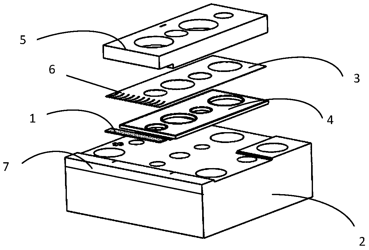
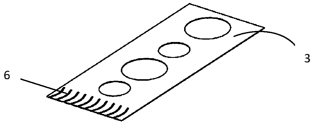
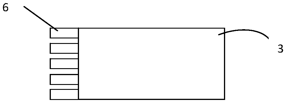
[0035] The high-power semiconductor laser of the present invention mainly includes a four-layer structure stacked in sequence. The first layer is a heat sink as a positive connection block. A chip mounting area and an insulating area are arranged on the mounting plane of the heat sink. The second layer includes a semiconductor laser A chip and an insulating sheet, the semiconductor laser chip is welded on the chip installation area, the insulating sheet is installed on the insulating area, the third layer is an electrode connection layer, and the fourth layer is a negative electrode connection block.

[0036] If the electrode connection layer is integrally welded with the semiconductor laser chip, the area in contact with the semiconductor laser chip is relatively large, and the semiconductor laser chip and the contacted electrode connection thin layer area are fixedly connected by solder. The solder layer is usually thick on both sides and thin in the middle. Due to the temper...


PUM


Abstract

The invention provides a high-power semiconductor laser unit of a low thermal stress structure. The high-power semiconductor laser unit of the low thermal stress structure has low thermal stress and can be adapted to complex working environments. The high-power semiconductor laser unit mainly comprises four structure layers which are stacked sequentially, the first layer is a heat sink serving as a positive electrode connection block, the installation plane of the heat sink is provided with a chip installation region and an insulating region, the second layer comprises a semiconductor laser unit chip and an insulating strip, the semiconductor laser unit chip is welded to the chip installation region, the insulating strip is installed in the insulating region, the third layer is an electrode connection layer playing a conductive role, and the fourth layer is a negative electrode connection block. In the electrode connection layer, the portion welded to the semiconductor laser unit chip is of a plane dentiform structure and used for reducing the thermal stress between the electrode connection layer and the chip, a gap is formed between the portion and the negative electrode connection block, and other portions of the electrode connection layer are welded to the negative electrode connection block.

Description

technical field [0001] The invention relates to a low stress semiconductor laser. Background technique [0002] The stress generated by semiconductor laser packaging seriously restricts the output optical power, working life and spectral characteristics of the device, which is the main factor causing the poor reliability of high-power semiconductor lasers. [0003] For semiconductor lasers, the main cause of thermal stress is the inconsistency of the thermal expansion coefficient (contact surface) between the positive and negative surfaces of the semiconductor laser chip and the corresponding conductive block (usually in the form of a connection layer or directly using a heat sink) caused by. Taking the positive side as an example, for good heat dissipation, the positive side of the semiconductor laser chip is usually welded to a metal heat sink with high thermal conductivity. Since the thermal expansion coefficients of the semiconductor laser chip and the heat sink are in...

Claims


Application Information

Patent Timeline
Patent Type & Authority Applications(China)
IPC IPC(8): H01S5/024H01S5/042
Inventor 刘兴胜王警卫
Owner FOCUSLIGHT TECH
Why Eureka
Try Eureka