
Pretreatment method of deep hole electroplating

A deep hole electroplating and pretreatment technology, applied in the direction of circuits, semiconductor devices, etc., can solve the problems that the air bubbles in the through holes cannot be completely removed, the difference in metal ion concentration, and the concentration of power lines, etc., so as to reduce the amount of residual gas, reduce air bubbles, and increase reliability. sexual effect

Active Publication Date: 2016-06-01
SHANGHAI JIAOTONG UNIV
View PDF2 Cites 0 Cited by
  • Summary
  • Abstract
  • Description
  • Claims
  • Application Information

AI Technical Summary

Problems solved by technology

Filling through holes by electroplating has advantages in cost and simple process, but for through holes with large aspect ratio, it is not easy to achieve defect-free filling in the hole
The main problems are: concentration of power lines at the orifice; differences in the concentration of metal ions at the orifice and the bottom of the through hole
The above process has a good impact on the filling effect of the through hole, but due to the large depth-width ratio of the through hole, it is difficult to fully contact the deep part of the through hole with the plating solution, and it is impossible to completely remove the bubbles in the deep part of the through hole to achieve no porosity filling

Method used


Image

  • Pretreatment method of deep hole electroplating
  • Pretreatment method of deep hole electroplating
  • Pretreatment method of deep hole electroplating

Examples


Embodiment 1

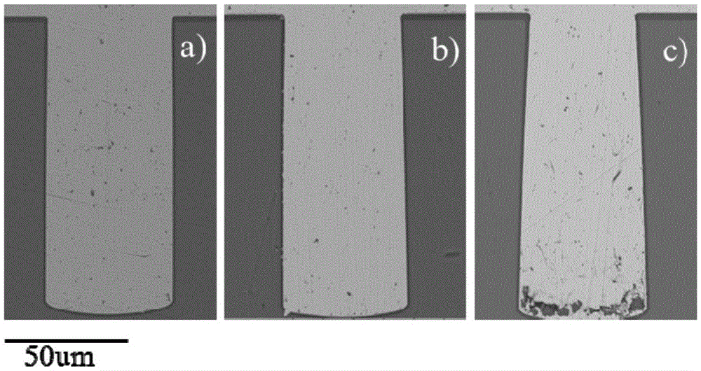
[0028] 1) Select the TSV chip with multiple 50×105um deep holes to be plated, select pure water, and cool to 10°C respectively;

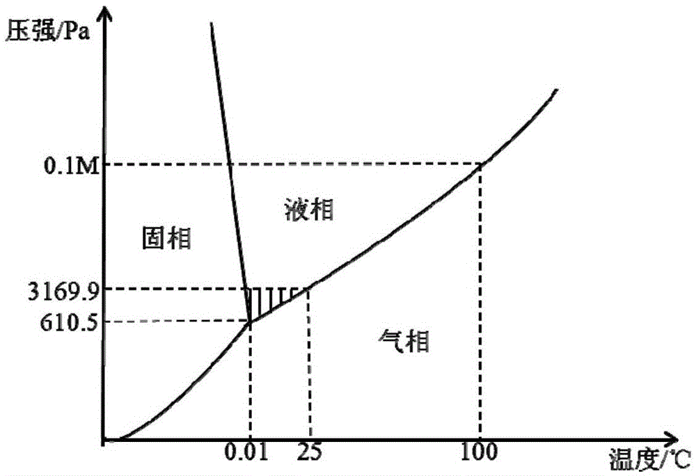
[0029] 2) Vacuumize the TSV chip for 15 minutes, and the vacuum degree is 610.5Pa;

[0030] 3) Soak the TSV chip in the pure water for 10 minutes under vacuum;

[0031] 4) Soak the TSV chip in a plating solution with a copper ion concentration of 40g / L, a hydrogen ion concentration of 10g / L, and a chloride ion concentration of 50ppm, 4ppmSPS, 300ppmPEG, and 100ppmJGB, while stimulating with a small current of 0.5ASD;

[0032] 5) Electroplating the TSV chip with the above plating solution for 2 hours, with an electroplating current density of 10ASD.

Embodiment 2

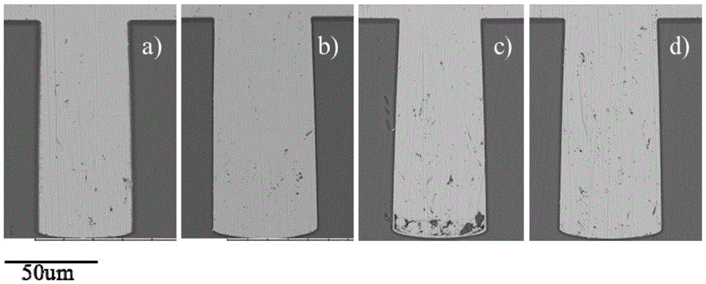
[0034] 1) Select 2 pieces of TSV chips with multiple 50×105um deep holes to be plated, select an appropriate amount of pure water, and cool the 2 pieces to 0°C;

[0035] 2) Vacuumize the TSV chips respectively for 10 minutes, and the vacuum degrees are 1000Pa and 2000Pa respectively;

[0036] 3) Soak the TSV chip in the pure water for 2 minutes under vacuum;

[0037] 4) Soak the TSV chip in a plating solution with a copper ion concentration of 40g / L, a hydrogen ion concentration of 10g / L, and a chloride ion concentration of 50ppm, 4ppmSPS, 300ppmPEG, and 100ppmJGB, while stimulating with a small current of 0.01ASD;

[0038] 5) The TSV chip was electroplated for 5 hours using the above plating solution, and the electroplating current density was 0.4ASD.

Embodiment 3

[0040] 1) Select two TSV chips with multiple 50×105um deep holes to be plated, select an appropriate amount of pure water, and cool to 15°C;

[0041] 2) Vacuumize the TSV chips respectively for 10 minutes, and the vacuum degrees are 1000Pa and 2000Pa respectively;

[0042] 3) Soak the TSV chip in the pure water for 2 minutes under vacuum;

[0043] 4) Soak the TSV chip in a plating solution with a copper ion concentration of 40g / L, a hydrogen ion concentration of 10g / L, and a chloride ion concentration of 50ppm, 4ppmSPS, 300ppmPEG, and 100ppmJGB, while stimulating with a small current of 0.01ASD;

[0044] 5) The TSV chip was electroplated for 5 hours using the above plating solution, and the electroplating current density was 0.4ASD.


PUM


Abstract

The invention relates to a pretreatment method of deep hole electroplating, which comprises the following steps that (1) a to-be-electroplated semiconductor chip provided with one or more deep holes is selected; pure water is selected and cooled; (2) the semiconductor chip is vacuumized; (3) the semiconductor chip is soaked in the pure water at vacuum; (4) the semiconductor chip is soaked by an electroplating solution and stimulated by low current; and (5) the semiconductor chip is electroplated by the electroplating solution. According to the method, the deep holes are sufficiently contacted with the electroplating solution, so that residual bubbles in the large-depth-width-ratio hole diameter are reduced, and defects such as gaps and joints are reduced effectively.

Description

technical field [0001] The invention belongs to the field of three-dimensional packaging of semiconductor chips, and in particular relates to a pretreatment method for deep hole electroplating. Background technique [0002] In the three-dimensional packaging of semiconductor chips, through-holes are used as the interconnection method is the mainstream direction of packaging, and the corresponding through-hole plating technology is the key to the development of three-dimensional packaging. Traditional through-hole plating is to achieve through-silicon hole filling by electroplating. Filling through holes by electroplating has advantages in cost and simple process, but for through holes with a large aspect ratio, it is not easy to achieve defect-free filling in the hole. The main problems are: concentration of power lines at the orifice; differences in the concentration of metal ions at the orifice and the bottom of the through-hole. Therefore, in the electroplating process,...

Claims


Application Information

Patent Timeline
Patent Type & Authority Patents(China)
IPC IPC(8): C25D5/00C25D7/12C25D7/04
Inventor 李明凌惠琴孙琪曹海勇李义
Owner SHANGHAI JIAOTONG UNIV
Learn More