Method for manufacturing super junction structure

A manufacturing method, N-type technology, applied in semiconductor/solid-state device manufacturing, electrical components, circuits, etc., can solve the problems of not being able to make full use of the chip area, not being able to be used as a current flow path, etc., to reduce the size of the cell, reduce the The effect of simple cost and process

Active Publication Date: 2014-04-16
XIAN LONTEN RENEWABLE ENERGY TECH +1
View PDF5 Cites 5 Cited by
  • Summary
  • Abstract
  • Description
  • Claims
  • Application Information

AI Technical Summary

Problems solved by technology

This process reduces the difficulty of forming P-columns, and can form narrow P-column regions. However, since the deep trenches are filled with insulating materials after implantation, this part cannot be used as a current flow path, and the chip area cannot be fully utilized.

Method used


Image

  • Method for manufacturing super junction structure
  • Method for manufacturing super junction structure
  • Method for manufacturing super junction structure

Examples


Embodiment Construction

[0025] The present invention will be described in detail below in conjunction with specific embodiments.

[0026] A method for manufacturing a super junction structure is achieved through the following steps:

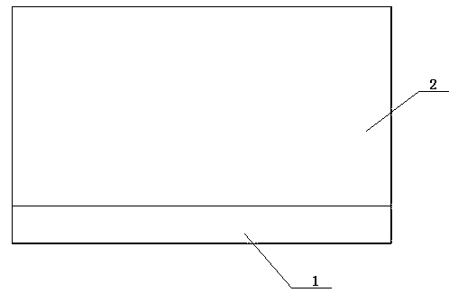
[0027] Step 1: Prepare an N-type heavily doped N+ substrate 1, and form a first N-type epitaxial layer on the N+ substrate 1, using the first N-type epitaxial layer as the N-type drift region 2, see figure 1 ;

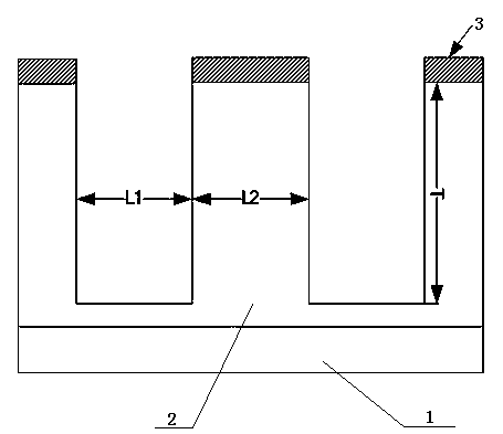
[0028] Step 2: Deposit a protective oxide layer on the upper surface of the N-type drift region 2 and define the trench etched area by photolithography; use an anisotropic etching method to etch the trench on the N-type drift region 2; wherein, The trench depth is T and smaller than the thickness of the N-type drift region 2, the trench width is L1, and the distance between adjacent trenches is L2, see figure 2 ;

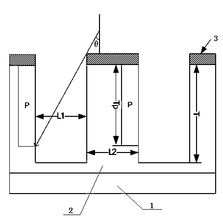
[0029] Step 3: Boron ions are implanted into the two sidewalls of the trench by side injection to form a P column region, the depth of the P column region i...


PUM


Abstract

The invention relates to a method for manufacturing a super junction structure. An existing method is complex in process and high in cost. The method for manufacturing the super junction structure is characterized by including the steps of preparing an N-type heavy doping N+ substrate and forming a first N-type epitaxial layer; depositing a protective oxide layer on the upper surface of an N-type drift region and defining a groove etching region; injecting boron ions to the two side walls of a groove to form a P post region; growing a second N-type epitaxial layer in the groove and on the upper surface of the N-type drift region, and growing a P-type epitaxial layer on the second N-type epitaxial layer to fill the groove; flattening and smoothening the upper surface. According to the method for manufacturing the super junction structure, a p post region and an n post region with a high depth-to-width ratio can be formed, a groove with a high depth-to-width ratio does not need to be etched, the process is simple, the cell size of a device can be effectively reduced, specific on-resistance is lowered, and cost is reduced.

Description

technical field [0001] The invention belongs to the technical field of semiconductors and relates to a method for manufacturing a super junction structure. Background technique [0002] Power semiconductor devices are widely used in power supplies or adapters of consumer electronics products such as mobile phones, computers, lighting and LCD TVs. Power mos devices also have the advantages of low input impedance and fast switching speed. In order to meet the requirements of withstand voltage, the MOS device needs to have a thick drift region and a low doping concentration of the drift region. The reduction of doping concentration in the drift region will increase the on-resistance and on-state loss of the device. [0003] The Super Junction structure uses an alternate PN junction structure instead of a single conductivity type material as the drift region, and a lateral electric field is introduced in the drift region, so that the device drift region can be completely deple...

Claims


Application Information

Patent Timeline
Patent Type & Authority Applications(China)
IPC IPC(8): H01L21/331H01L21/265
CPCH01L29/0634
Inventor 陈桥梁张园园马治军倪嘉
Owner XIAN LONTEN RENEWABLE ENERGY TECH
Why Eureka
Try Eureka