Cuprous sulfide nano ring structure semiconductor material and preparation method thereof

A ring structure, cuprous sulfide technology, applied in the direction of copper sulfide, nanotechnology, nanotechnology, etc., can solve the problems of non-repeatability, limited application, complexity, etc., and achieve low growth temperature, high repeatability, and low cost Effect

Inactive Publication Date: 2014-04-23
EAST CHINA NORMAL UNIV
View PDF3 Cites 7 Cited by
  • Summary
  • Abstract
  • Description
  • Claims
  • Application Information

AI Technical Summary

Problems solved by technology

However, its most important preparation method still has defects such as complexity, non-...

Method used


Image

  • Cuprous sulfide nano ring structure semiconductor material and preparation method thereof
  • Cuprous sulfide nano ring structure semiconductor material and preparation method thereof
  • Cuprous sulfide nano ring structure semiconductor material and preparation method thereof

Examples


Embodiment Construction

[0020] The present invention will be further described in detail in conjunction with the following specific embodiments and accompanying drawings. The process, conditions, reagents, experimental methods, etc. for implementing the present invention are general knowledge and common knowledge in the art except for the content specifically mentioned below, and the present invention has no special limitation content.

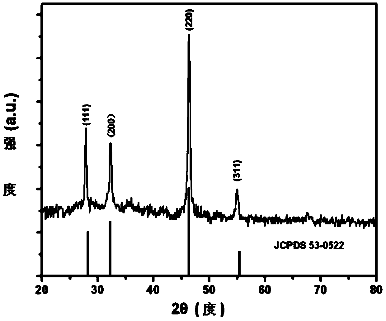
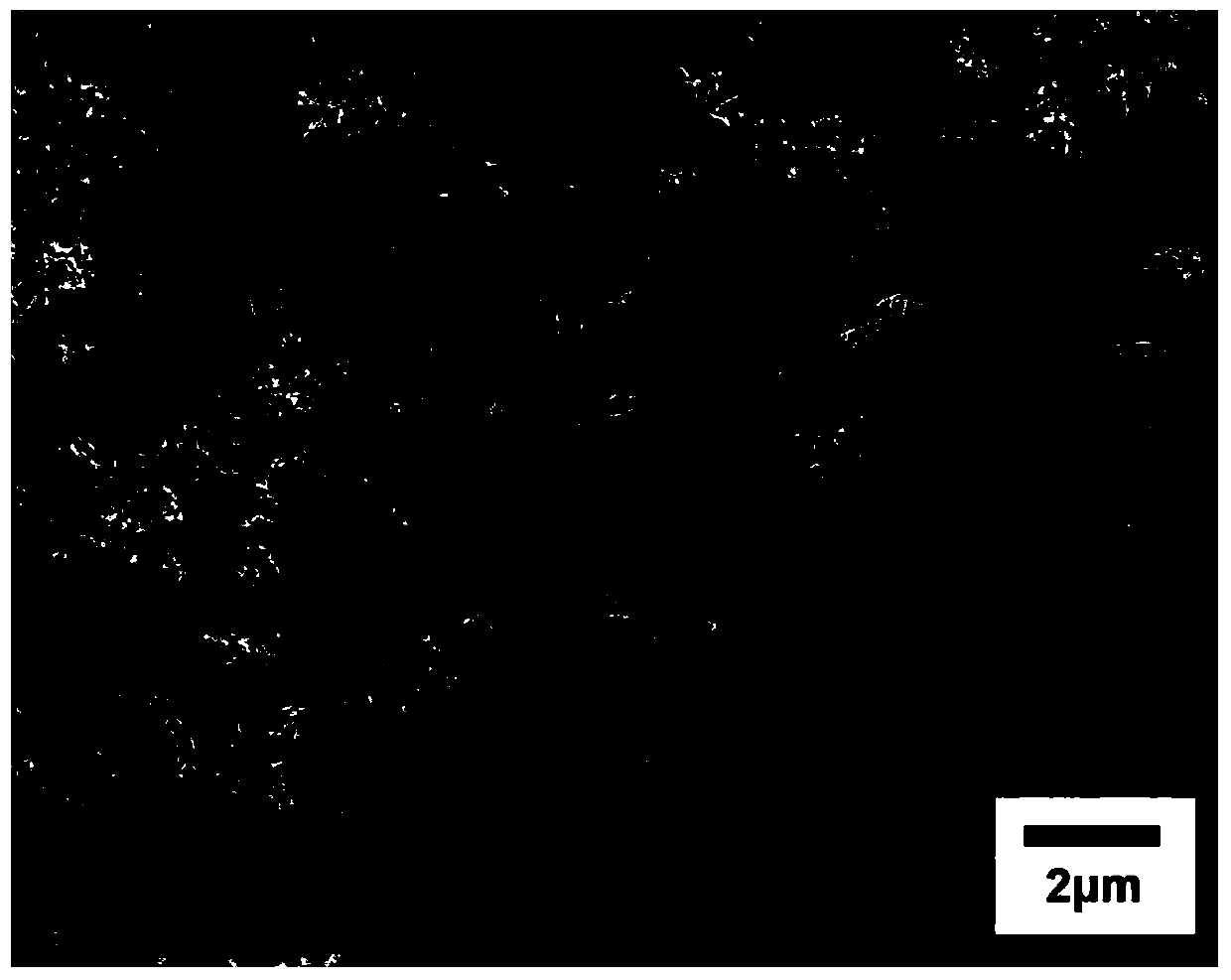
[0021] The specific preparation steps of cuprous sulfide micron ring semiconductor material in the present embodiment are as follows:

[0022] a. Mix 36ml of absolute alcohol with 4ml of deionized water to make 40ml of a specific solution.

[0023] b. Divide the prepared 40ml solute into two parts and put them into clean beakers respectively.

[0024] c. Put 0.6g CuCl into 20ml solute and mix evenly, put 0.8g thiourea into 20ml solute and mix evenly.

[0025] d. Mix the completely mixed 20ml CuCl solution and 20ml thiourea solution, and stir on a magnetic stirrer f...


PUM


Abstract

The invention discloses a cuprous sulfide micron ring structure semiconductor material comprising a hierarchical structure consisting of sheets and a porous ring structure consisting of particles. The invention also discloses a preparation method of the cuprous sulfide micron ring structure semiconductor material, and the preparation method comprises the steps of mixing anhydrous ethanol with deionized water to prepare a mixed solution, preparing a thiourea solution and a CuCl solution respectively, and uniformly mixing; adding the mixture into a reaction kettle, sealing the kettle, reacting for 5 hours at 150 DEG C; after the reaction, putting the reactant on a silicon chip, and baking at 55 DEG C to obtain the cuprous sulfide micron ring structure semiconductor material. The cuprous sulfide micron ring structure semiconductor material disclosed by the invention has the advantages of low cost, relatively low growth temperature and relatively high repeatability, and has great potential in the aspects of photo-catalysis of industrial polluted wastewater and field emission luminescence.

Description

technical field [0001] The invention relates to the technical field of optoelectronic materials, semiconductor materials and devices, in particular to a cuprous sulfide micron ring-structured semiconductor material and a preparation method thereof. Background technique [0002] Cu 2 S is a P-type narrow bandgap semiconductor material with a direct bandgap of 1.2eV and excellent electrical conductivity. Because of its unique electrical, chemical and optical properties, Cu 2 S has a wide range of research and applications in the fields of solar cells, photocatalysis, field emission, and sensors. Existing literature reports the preparation of one-dimensional and two-dimensional cuprous sulfide semiconductor materials, such as: nanoparticles, nanorods, nanowires, nanotubes, and nanocolored ribbons; three-dimensional nanostructures, such as: nanospheres, nanoflowers, etc., also was successfully prepared. However, the preparation of cyclic cuprous sulfide semiconductor materia...

Claims


Application Information

Patent Timeline
IPC IPC(8): C01G3/12B82Y30/00B82Y40/00
Inventor 赵彬郁可李守川朱自强
Owner EAST CHINA NORMAL UNIV
Why Eureka
Try Eureka