

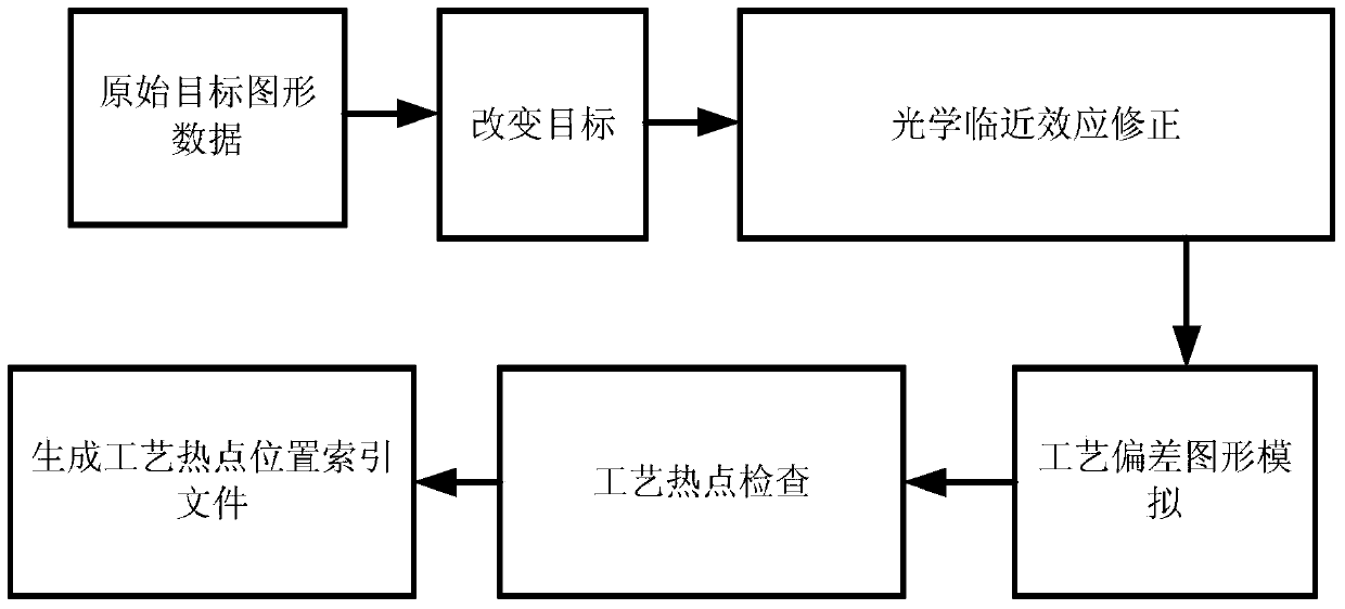
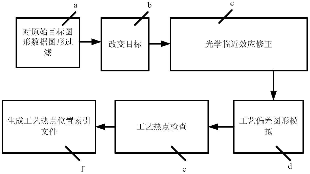
Layout design photoetching technology friendliness detection method based on regular figure filtering
A lithography process and layout design technology, which is applied in the direction of photolithography process exposure device, microlithography exposure equipment, etc., can solve the problem of unfavorable layout design, lithography process friendliness check kit application, software calculation and long use time, production cost Advanced problems, to achieve good matching, fast and accurate search, and reduce the cost of use
- Summary
- Abstract
- Description
- Claims
- Application Information
AI Technical Summary
Problems solved by technology
Method used
Image

Examples
Embodiment 1
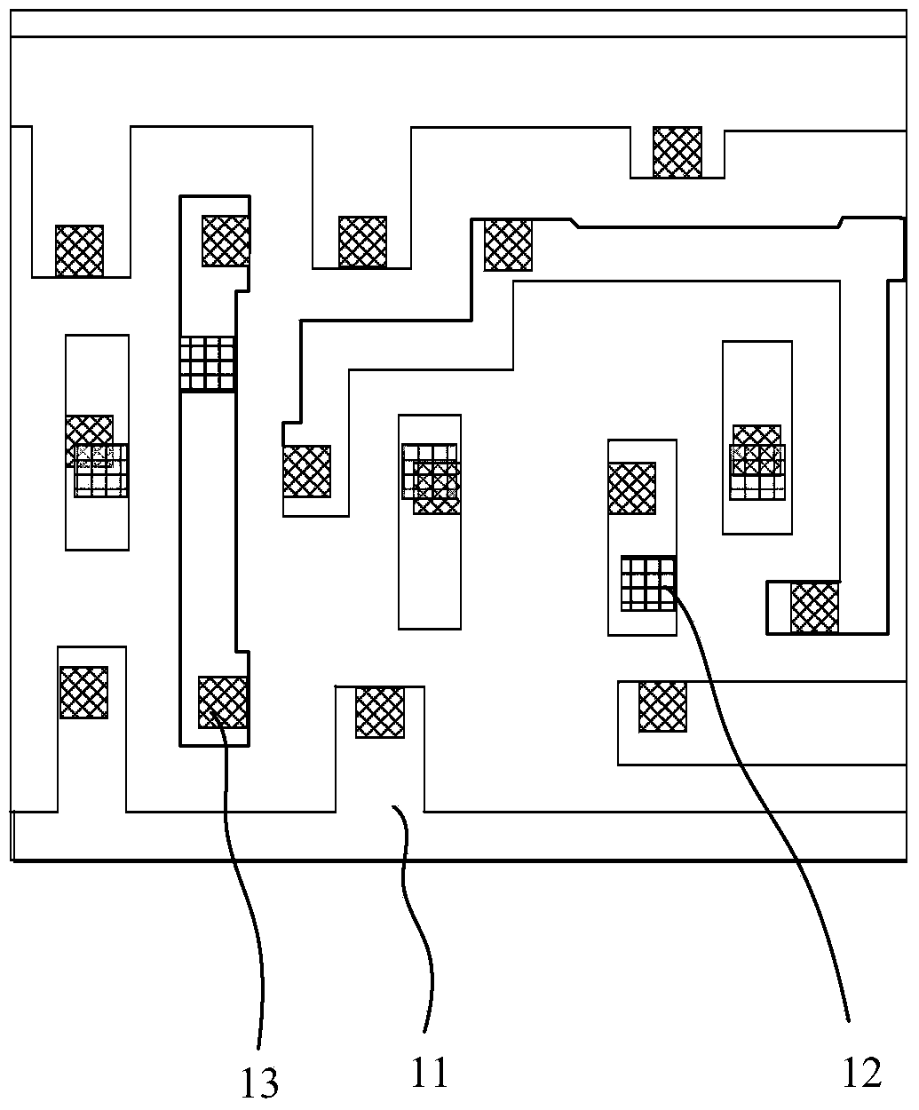
[0044] Figure 3(a) ~ Figure 3(f) An embodiment of filtering the original target graphic data in the layout design lithography process friendliness inspection method based on regular graphic filtering of the present invention, combined with Figure 3(a) ~ Figure 3(f), this embodiment is a method for filtering the original data by using the graphics around the edge fragment near the convex corner vertex in the original target graphic data, the filtering method described in this embodiment can be used to find the clip Potential process hot spots such as Line Pinch, Line Bridge and Hole Overlap Missing.
[0045] For example, filtering raw target pattern data to find potential process hotspots with bad connections. FIG. 3( a ) is a design pattern of part M1 (first metal wiring), including a first connection layer ( M1 ) 11 , a contact hole ( CONTACT ) 12 and a first via layer ( VIA1 ) 13 . As shown in Figure 3(b), select all the cut edges 14 of the vertices of the convex corners...
Embodiment 2
[0047] Figure 4(a) ~ Figure 4(e) Another embodiment of filtering the original target graphic data in the method for checking the friendliness of the layout design lithography process based on regular graphic filtering in the present invention, combined with Figure 4(a) ~ Figure 4(e) , this embodiment is a method of filtering the original target graphic data by using the graphics around the edge fragment near the concave corner vertex. This method can be used to find the line pinch (Line Pinch) and line connection (Line Bridge) And other types of process hotspots.
[0048] FIG. 4(a) is a design pattern of a small part of M1 (first metal wiring), including the first connection layer 11 (M1). As shown in Fig. 4 (b), first select all trimmings 22 near the apex of the concave angle, wherein the length of the trimmings 22 can be 0.5 times the minimum design size of the gap (space), preferably 0.4 to 0.45 times, This keeps two adjacent cut edges from spanning the entire gap width...
Embodiment 3
[0050] Figure 5(a) ~ Figure 5(g) Another embodiment of filtering the original target graphic data in the layout design lithography process friendliness inspection method based on regular graphic filtering of the present invention, combined with Figure 5(a) ~ Figure 5(g) In this embodiment, the method of filtering the original data by using the graphics around the edge fragment near the apex of the concave angle can be used to find the unevenness of the channel length or channel width of the transistor due to the L-shaped design of the short extension A filtering method for potential process hotspot areas, which will affect the electrical performance of the device or even fail, especially for short-channel transistors.
[0051] FIG. 5( a ) is a plane design of a small part of transistors, including a polycrystalline layer (Poly) 31 and an active area (Active Area) 32 . As shown in FIG. 5( b ), the gate region 33 is selected first, wherein the width of the active region is ca...
PUM
 Abstract
Description
Claims
Application Information