Manufacturing method of multi-channel light filtering micro lens array

A technology of microlens array and manufacturing method, applied in the field of optical devices, to achieve monochrome imaging and color reconstruction, compact structure, and miniaturization

Active Publication Date: 2014-04-30
GUANGZHOU INST OF ADVANCED TECH CHINESE ACAD OF SCI
5 Cites 16 Cited by

AI-Extracted Technical Summary

Problems solved by technology

[0005] In order to solve the above problems, the present invention provides a method for manufacturing a multi-channel filter microlens array that greatly r...

Method used

5. then the substrate 1 that is plated with chromium film 5 is placed in acetone, the AZ4620 positive photoresist 2 that is not exposed on substrate 1 can be dissolved in acetone, and the chromium film 5 that is plated on it is also simultaneously After being stripped and removed, 9 light-transmitting light-transmitting holes 51 are exposed on the chromium film 5, and these 9 light-transmitting light-transmitting holes 51 will be used to make 9 different filter layers 8 in subsequent steps. The light-transmitting holes 51 Surrounding it is a layer of opaque chromium film 5, which can block the incident of stray light.
8. After exposure, substrate 1 is placed in developing solution for development, removes unexposed photoresist 6, then bakes in oven to further cure photoresist 6, improves the stability of photoresist 6, bakes The baking temperature is 230 degrees centigrade, and the time is 1 hour. After the photoresist 6 is baked and cured, a filter layer 8 of a certain color (such as red) is made at a light transmission hole 51 .
In the manufacture method of this multi-channel filter microlens array, with the photoresist 6 of different colors, on substrate 1, make the filter layer 8 with filter function in conjunction with traditional photolithography, then directly in The convex microlens 10 array is made by hot-melting method at the 8 places of the filter layer, so that the convex microlens integrates the filtering function without additional filter structure, ...

Abstract

The invention discloses a manufacturing method of a multi-channel light filtering micro lens array. According to the manufacturing method of the multi-channel light filtering micro lens array, due to the facts that a light filtering layer with the light filtering function is manufactured on a substrate by using photoresist with different colors and combining a traditional photoetching method, and then the micro convex lens array is directly manufactured on the light filtering layer through a hot melting method, the purpose that micro convex lenses have the integrated light filtering function can be achieved, additional optical filter structures are not needed, and development of the compact multi-channel light filtering micro lenses is achieved; a plurality of optical channels are arranged, and each optical channel can independently obtain image information of the corresponding wave band; due to the facts that the photoetching technology is adopted, and a first mask plate is used in cooperation, alignment between optical filters and the micro lens array is avoided; due to the fact that a light barrier layer is additionally arranged between every two adjacent micro convex lenses on the substrate, influence caused by incident stray light on the micro lenses can be reduced; the micro convex lens array can be applied to a multispectral imaging system, and monochrome imaging and color reconstruction are achieved; meanwhile, the micro convex lens array is compact in structure, and miniaturization of the multispectral imaging system is facilitated.

Application Domain

Technology Topic

Image

  • Manufacturing method of multi-channel light filtering micro lens array
  • Manufacturing method of multi-channel light filtering micro lens array

Examples

  • Experimental program(1)

Example Embodiment

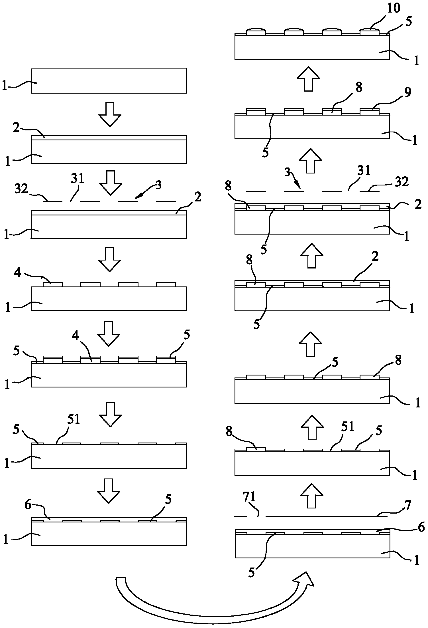
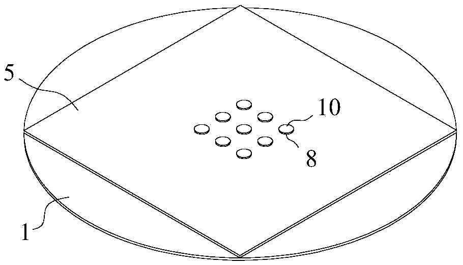
[0023] refer to figure 1 , figure 2 , The invention provides a manufacturing method of a multi-channel filter microlens array, compared with the traditional microlens array, it can filter and condense light of several different spectra at the same time. The set of microlenses is applied in a multispectral imaging system to realize monochrome imaging and color reconstruction. In this way, one filter structure can be reduced compared with the traditional multispectral imaging system, and the problem of alignment between the filter and the microlens array is avoided. This method mainly comprises the following steps:
[0024] 1. Take a glass sheet with a flat surface and high light transmittance as substrate 1. After cleaning the substrate with water and acetone, place it in an oven and bake it at 130°C for 10 minutes to remove water vapor and residual acetone. After natural cooling, the AZ4620 positive photoresist 2 was spin-coated on the substrate 1, and the spin coating parameters were 500 rpm for 10 seconds and 2500 rpm for 30 seconds. At this time, the thickness of the AZ4620 positive photoresist 2 was 10 Microns or so.
[0025] 2. Bake the substrate 1 spin-coated with AZ4620 positive photoresist 2 on a baking table at 90°C for 1 minute to remove the solvent in the AZ4620 positive photoresist 2. After baking, UV exposure was performed on the pre-made first mask plate 3, the exposure time was 25 seconds, and the exposure intensity was 20mW/cm 2. The first mask 3 includes a light-transmitting area 31 and nine opaque areas 32 (circular) located in the middle of the light-transmitting area.
[0026] 3. After the exposure is complete, place the substrate 1 in a developer solution for development. The AZ4620 positive photoresist 2 facing the light-transmitting area 31 of the first mask 3 is exposed and dissolved and removed under the developing solution, and the AZ4620 positive photoresist facing the opaque area 32 of the first mask 3 2 is retained without being exposed; the developer type is AZ400, after development, nine cylindrical patterns 4 will be revealed, and the surrounding AZ4620 positive photoresist 2 will be removed during development due to exposure.
[0027] 4. Place the developed substrate 1 in the sputter ion coating machine for coating, and coat the substrate 1 with a layer of opaque chromium (Cr) film 5 as a light blocking layer. Because the AZ4620 positive photolithography produced before For the protection of the glue 2, the chrome film 5 is only plated at the 9 cylindrical patterns 4.
[0028] 5. Then place the substrate 1 coated with the chromium film 5 in acetone, the unexposed AZ4620 positive photoresist 2 on the substrate 1 will be dissolved in the acetone, and the chromium film 5 plated on it will be stripped and removed at the same time At this moment, nine light-transmitting light-transmitting holes 51 are exposed on the chrome film 5, and these nine light-transmitting light-transmitting holes 51 will be used for making nine different filter layers 8 in the follow-up, surrounded by a circle of light-transmitting holes 51. Layer opaque chromium film 5 can play the purpose of blocking the incident of stray light.
[0029] 6. Spin-coat the photoresist 6 of one color (such as red) on the substrate 1 with 9 light-transmitting holes 51, the spin-coating parameter is 550 rpm for 30 seconds, and the thickness of the photoresist 6 is about 1 micron , after spin coating, the substrate 1 was placed in an oven and baked at 88oC for 4 minutes to remove the solvent in the photoresist 6 .
[0030] 7. After drying, put it under the second mask plate 7 for ultraviolet exposure, the exposure dose time is 12 seconds, and the exposure intensity is 20mW/cm 2 , the photoresist 6 is a negative photoresist, the properties of the exposed photoresist 6 will change and cannot be dissolved in the developer solution, wherein the second mask plate 7 includes a light-tight plate, which is light-tight A through hole 71 corresponding to any light transmission hole 51 is provided on the board.
[0031] 8. After the exposure is complete, place the substrate 1 in a developer for development, remove the unexposed photoresist 6, and then bake in an oven to further cure the photoresist 6 to improve the stability of the photoresist 6. The baking temperature is 230 degrees Celsius, the time is 1 hour, after the photoresist 6 is baked and cured, a filter layer 8 of a certain color (such as red) is made at a light transmission hole 51 .
[0032] 9. Repeat steps 6-8 to make filter layers 8 of other colors at other light transmission holes 51. The filter layer 8 includes a red filter layer, an orange filter layer, a yellow A filter layer, a green filter layer, a blue filter layer, a blue filter layer, a purple filter layer, a near-infrared filter layer and a visible light filter layer. Among them, red, green, blue, and yellow photoresists can be purchased from merchants, and the red filter layer, green filter layer, blue filter layer, and yellow filter layer are directly photolithographically etched by photoresists of corresponding colors. Formation; the orange filter layer is formed by mixing red photoresist and blue photoresist at a volume ratio of 1:1; the cyan filter layer is formed by volume ratio of blue photoresist and green photoresist It is formed by photolithography after mixing ratio 1:1; the purple filter layer is formed by photolithography after mixing red, blue and green photoresists in a volume ratio of 1:1:0.2; the near-infrared filter layer is formed by sequentially mixing red, green And the blue photoresist is made in the same area through three photolithography; the visible light filter layer does not need photoresist.
[0033] 10. AZ4620 positive photoresist 2 is spin-coated on the outside of the filter layer 8 on the substrate 1. The AZ4620 positive photoresist 2 needs a certain thickness, which is realized by two times of glue-spinning process. Spin coating at 1200 rpm for 45 seconds each time, followed by 30 seconds at 2000 rpm; after the first spin, bake at 85 oC on a baking table for 2 Minutes, and then continue to shake the second layer of glue. After spinning the glue twice, the coating thickness of the AZ4620 positive photoresist 2 is about 20-23 microns.
[0034] 11. Put the substrate 1 spin-coated with AZ4620 positive photoresist 2 in an oven and bake at 85 oC for 8 minutes to completely remove the solvent in AZ4620 positive photoresist 2.
[0035] 12. After drying, place the substrate 1 under the first mask 3 for ultraviolet exposure. The 9 opaque regions 32 on the first mask 3 correspond to the 9 filter layers 8, and the exposure time is 12-14 seconds, the exposure intensity is about 20mW/cm 2.
[0036] 13. Put the exposed substrate 1 into the AZ400 developer for development, the exposed AZ4620 positive photoresist 2 will be dissolved and removed under the developer, while the unexposed AZ4620 positive photoresist 2 will remain and be removed. A plurality of AZ4620 cylindrical bosses 9 are formed on the surface of the substrate 1 . If the development cannot be completely developed to the end, 2-3 microns of AZ4620 positive photoresist 2 should be reserved, which is conducive to the formation of a lens spherical surface by the AZ4620 positive photoresist 2 under the action of surface tension in the subsequent hot-melt process. The degree of development can be controlled by developing multiple times and measuring the height of the cylinder with a step meter, so as to ensure that the height of the finally obtained cylindrical boss 9 is about 20 microns. After the development is completed, the remaining developer solution on the substrate is washed with deionized water, and then blown dry with nitrogen gas.
[0037] 14. Place the substrate 1 on a baking table at 128 oC, heat-fuse for 115 seconds, and the AZ4620 cylindrical boss 9 will form a convex microlens 10 under the action of surface tension.
[0038] In the manufacturing method of this multi-channel filter microlens array, photoresists 6 of different colors are used in combination with traditional photolithography to make a filter layer 8 with a filter function on the substrate 1, and then directly on the filter layer 8. The array of convex microlenses 10 is made by thermal fusion at layer 8, so that the convex microlenses integrate light filtering function without additional filter structure, and the development of compact multi-channel light filtering microlenses is realized. The invention has a plurality of optical channels, and each channel can independently acquire image information of a corresponding waveband. Due to the use of photolithography technology and the cooperation with the first mask plate 3 , the problem of alignment between the filter and the microlens array is also avoided. In addition, a layer of light blocking layer is added between the convex micro-lenses on the substrate 1, which can reduce the impact between incident stray light and the lenses. The convex microlens array can be applied to a multispectral imaging system to realize monochromatic imaging and color reconstruction; meanwhile, the convex microlens array has a compact structure, which is also beneficial to the miniaturization of the multispectral imaging system.
[0039] Of course, the present invention is not limited to the above-mentioned embodiments. Those skilled in the art can also make equivalent modifications or replacements without violating the spirit of the present invention. These equivalent modifications or replacements are all included in the claims of this application. within a limited range.

PUM

no PUM

Description & Claims & Application Information

We can also present the details of the Description, Claims and Application information to help users get a comprehensive understanding of the technical details of the patent, such as background art, summary of invention, brief description of drawings, description of embodiments, and other original content. On the other hand, users can also determine the specific scope of protection of the technology through the list of claims; as well as understand the changes in the life cycle of the technology with the presentation of the patent timeline. Login to view more.

Similar technology patents

Floating keyboard

InactiveUS20060210340A1Alleviates repetitive stress injuryReduce the impactInput/output for user-computer interactionCathode-ray tube indicatorsAmbulation DevicesEngineering
Owner:ERGOWERX

Combination of sulfonamide compound and tafluprost

InactiveUS20140018350A1Good effectReduce the impactBiocideOintment deliveryTherapy medicationBenzyl group
Owner:SANTEN PHARMA CO LTD +1

Classification and recommendation of technical efficacy words

Why Eureka
Try Eureka