Electronic equipment and manufacturing method for single-layered multipoint capacitive touch screen and touch layer

A capacitive touch screen, single-layer multi-point technology, applied in electrical digital data processing, data processing input/output process, instruments, etc. problems, to improve the reliability of types and use, improve the range of types and applications, and achieve good anti-interference performance.

Inactive Publication Date: 2014-04-30
SHENZHEN SUCCESS ELECTRONICS LTD
View PDF9 Cites 7 Cited by
  • Summary
  • Abstract
  • Description
  • Claims
  • Application Information

AI Technical Summary

Problems solved by technology

This has brought a series of problems, such as high equipment investment, large workshop area, high energy consumption, and the development and etching process requires a large amount of acid and alkali, which is not conducive to environmental protection
At the same time, indium tin oxide is a rare earth oxide, and its resources are on the verge of depletion, and the conductive film made of this material has a relatively high impedance. For a large-sized touch screen, its touch accuracy and sensitivity are difficult to meet the requirements.
[0004] There are also some companies or research institutions in the industry that have published methods for making touch screens with ITO (indium tin oxide) alternative materials, such as carbon nanotubes, metal grids, nano silver wires, conductive polymer materials, etc., but either the material preparation is difficult, or It is difficult to manufacture conductive film or conductive pattern, the process is complicated, and it is difficult to industrialize

Method used


Image

  • Electronic equipment and manufacturing method for single-layered multipoint capacitive touch screen and touch layer
  • Electronic equipment and manufacturing method for single-layered multipoint capacitive touch screen and touch layer
  • Electronic equipment and manufacturing method for single-layered multipoint capacitive touch screen and touch layer

Examples


Embodiment Construction

[0029] In order to make the object, technical solution and advantages of the present invention more clear, the present invention will be further described in detail below in conjunction with the accompanying drawings and embodiments. It should be understood that the specific embodiments described here are only used to explain the present invention, not to limit the present invention.

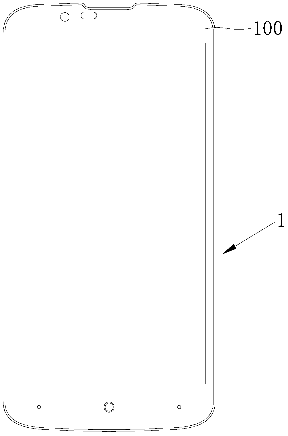
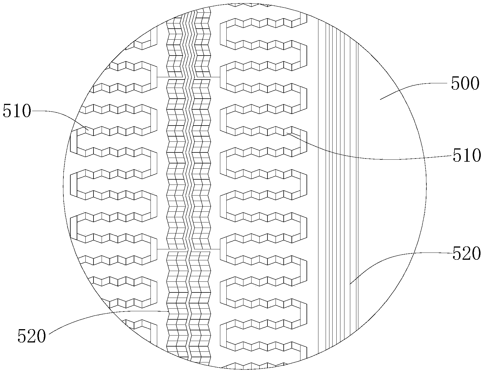
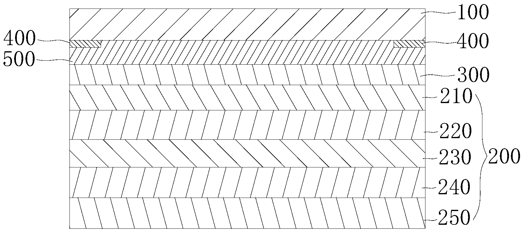
[0030] Such as Figure 1 to Figure 3 As shown, a single-layer multi-point capacitive touch screen 1 provided by the embodiment of the present invention includes a panel 100 for press touch and a screen module 200, and a transparent optical adhesive layer 300 is arranged between the panel 100 and the screen module 200 , the transparent optical adhesive layer 300 can also play the role of pasting the panel 100 on the screen module 200 under the condition of ensuring the light transmittance. Protect. A BM frame layer 400 (BM: an abbreviation of Black Matrix, which means black matrix in Chinese) i...


PUM


Abstract

The invention discloses electronic equipment and a manufacturing method for a single-layered multipoint capacitive touch screen and a touch layer thereof. The single-layered multipoint capacitive touch screen comprises a panel and a screen module, wherein a transparent optical adhesive layer is arranged between the panel and the screen module; a BM (basement membrane) frame layer is arranged on the frame of the panel; the screen module comprises an upper polaroid, an upper glass substrate, a lower glass substrate, a lower polaroid and a backlight plate which are sequentially arranged in a stacked manner from top to bottom and are adhered to one another; a metal conductive ink circuit layer is arranged between the panel and the screen module or in the screen module and comprises a plurality of touch units which are arranged in parallel; and each touch unit is independently provided with a lead connected with a processor. The single-layered multipoint capacitive touch screen is sensitive in touch, high in accuracy and wide in application range; the manufacturing method for the touch layer of the single-layered multipoint capacitive touch screen is simple; the touch layer is low in cost, and is energy-saving and environment-friendly; and the using convenience and the reliability of the electronic equipment with the touch screen are improved.

Description

technical field [0001] The invention belongs to the technical field of touch screen structures, and in particular relates to a single-layer multi-point capacitive touch screen, a manufacturing method of a touch layer, and an electronic device with the touch screen. Background technique [0002] The capacitive touch screen uses the current induction change of the human body to locate the touch position when touching. Touch technology of single-layer multi-point projected capacitive panel: single-layer multi-point projected capacitive touch screen is to etch ITO conductive circuit modules in different directions on a layer of ITO (indium tin oxide) conductive glass coating. The graphics etched on the two modules can be regarded as sliders that change continuously in the X and Y directions. Since the X and Y structures are on different surfaces, their intersections form a capacitor node. One slider can be used as a drive line, and the other slider can be used as a sense line....

Claims


Application Information

Patent Timeline
Patent Type & Authority Applications(China)
IPC IPC(8): G06F3/044
Inventor 杨顺林陈志雄廖昌朱少良
Owner SHENZHEN SUCCESS ELECTRONICS LTD
Why Eureka
Try Eureka