Method for manufacturing novel Damascus copper and copper bonding structure

A technology of Damascus copper and its production method, which is applied in the manufacture of semiconductor/solid-state devices, electrical components, electrical solid-state devices, etc. requirements, etc.

Active Publication Date: 2014-04-30
NAT CENT FOR ADVANCED PACKAGING
View PDF6 Cites 9 Cited by
  • Summary
  • Abstract
  • Description
  • Claims
  • Application Information

AI Technical Summary

Problems solved by technology

Limited by the height of the micro-bumps, the thickness of the photoresist is relatively large, which leads to the insufficient capability of the traditional micro-bump manufacturing process in the production of small-sized micro-bumps
In addition, the copper-copper bonding process has almost strict requirements on the flatness of the bonding interface, and the electroplating process cannot meet its requirements
First of all, the surface roughness of the copper pillars produced by the electroplating process is relatively large, which cannot meet the requirements of copper-copper bonding for surface flatness; secondly, the flatness of the micro-bumps produced by the electroplating process is poor, especially when there are steps in the lower layer , it is difficult to ensure the flatness of the micro-bump surface; third, the height of the micro-bumps in different regions of the wafer will have a large difference with the micro-bump technology of the traditional process, which will affect the bonding quality; fourth, the bottom of the traditional process Filling technology has been difficult to meet the fine-pitch, large-area chip micro-assembly process, the existing fine-pitch, large-area chip micro-assembly process is complicated, and its process reliability is low

Method used


Image

  • Method for manufacturing novel Damascus copper and copper bonding structure
  • Method for manufacturing novel Damascus copper and copper bonding structure
  • Method for manufacturing novel Damascus copper and copper bonding structure

Examples


Embodiment Construction

[0031] A method for manufacturing a new type of Damascus copper-copper bonding structure is characterized in that it comprises the following steps:

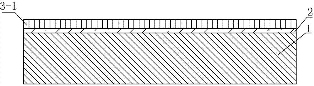
[0032] see figure 1 , (1) Make adhesion layer 2 and seed layer 3-1 on the surface of wafer 1. The material of the adhesion layer can be one or more of titanium, titanium nitride, tantalum, tantalum nitride, etc. The seed layer The material is copper. (The devices and interconnect structures have been fabricated on the wafer);

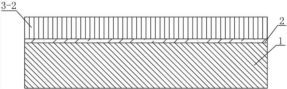
[0033] see figure 2 , (2) Depositing a copper layer 3-2 on the surface of the wafer by an electroplating process, the thickness of the copper layer is 1-15μm;

[0034] see image 3 , (3) Use photolithography to pattern the surface of the copper layer;

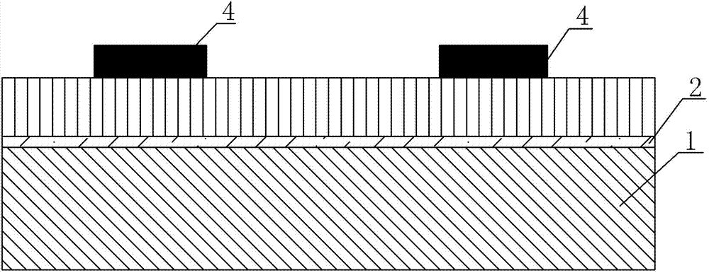
[0035] see Figure 4 , (4) Use an electrolysis process to remove the copper outside of the microbump position, and form a microbump structure 5 on the wafer. This process connects the copper on the wafer with the anode of the power supply. Generally, an acidic el...


PUM

PropertyMeasurementUnit
thicknessaaaaaaaaaa

Abstract

The invention provides a method for manufacturing a novel Damascus copper and copper bonding structure. The surface roughness of a copper cylinder is effectively reduced, the surface evenness of micro convex points is improved, the heights of the micro convex points in different areas of a wafer can be the same, the requirement for the surface evenness of the copper and copper bonding technology is met, the bottom filling technology is not needed in the following micro packaging technology, and the reliability of the bonding structure is improved while the technology complexity is reduced. The method is characterized by comprising the following steps that firstly, an adhesion layer and a seed layer are manufactured on the surface of the wafer; secondly, a copper layer is deposited on the surface of the wafer; thirdly, the copper layer is imaged; fourthly, copper not located in the micro convex point area is removed to form a micro convex point structure; fifthly, the adhesion layer not in the micro convex point area is removed to form an electric isolated micro convex point structure; sixthly, photoresist is removed to form a micro convex point structure; seventhly, parts between the micro convex points are filled and coated with a dielectric layer; eighthly, the surface of the wafer is processed to obtain highly-even dielectric layer with the flat and smooth surface and exposed micro convex point structures.

Description

Technical field [0001] The invention relates to the technical field of microelectronic packaging, in particular to a method for manufacturing a new type of Damascus copper-copper bonding structure. Background technique [0002] The current micro-bump manufacturing process uses photoresist to define the electroplating area after the seed layer is manufactured. Limited by the height of the micro bumps, the thickness of the photoresist is relatively large, which leads to insufficient capabilities in the production of small-size micro bumps in the traditional micro bump manufacturing process. In addition, the copper-copper bonding process has almost harsh requirements for the flatness of the bonding interface, and the electroplating process cannot meet its requirements. First, the surface roughness of the copper pillar produced by the electroplating process is relatively large, which cannot meet the requirements of copper-copper bonding for surface flatness; secondly, the flatness o...

Claims


Application Information

Patent Timeline
Patent Type & Authority Applications(China)
IPC IPC(8): H01L21/768
CPCH01L24/11H01L24/14H01L2224/11H01L2224/11602
Inventor 薛恺于大全
Owner NAT CENT FOR ADVANCED PACKAGING
Why Eureka
Try Eureka