An organic electroluminescent device

An electroluminescent device and luminescence technology, which is applied in the direction of electric solid devices, electrical components, semiconductor devices, etc., can solve the problems of difficult adjustment of viewing angle and low lifespan, and achieve the effects of excellent viewing angle, prolonging lifespan, and increasing the composite area

Active Publication Date: 2016-08-17
KUNSHAN NEW FLAT PANEL DISPLAY TECH CENT +1
View PDF5 Cites 0 Cited by
  • Summary
  • Abstract
  • Description
  • Claims
  • Application Information

AI Technical Summary

Problems solved by technology

[0009] For this reason, what the present invention is to solve is the problem that the viewing angle of the existing top-emitting blue light organic electroluminescent device is difficult to adjust and the service life is low, and a long-life blue top-emitting organic electroluminescent device with an excellent viewing angle is provided.

Method used


Image

  • An organic electroluminescent device
  • An organic electroluminescent device
  • An organic electroluminescent device

Examples


Embodiment 1

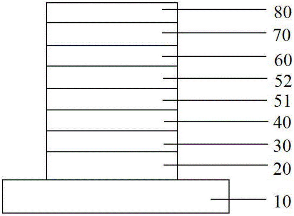
[0035] This embodiment provides an organic electroluminescent device, such as figure 1 As shown, the first electrode 20 , the blue light emitting layer and the second electrode 70 are sequentially stacked on the substrate 10 . The light emitting layer includes a first light emitting layer 51 and a second light emitting layer 52 stacked in sequence, and the first light emitting layer 51 is disposed close to the first electrode 20 . The first light-emitting layer 51 is a single hole-type host material-doped guest dye layer, the second light-emitting layer 52 is an electron-type host material-doped guest dye layer, and the thickness of the first light-emitting layer can be adjusted. The total thickness of the light emitting layer and the second light emitting layer is between 10nm and 40nm, wherein the thickness of the first light emitting layer is 1nm to 25nm.

[0036] The substrate 10 is selected from, but not limited to, a glass substrate and a polymer substrate. In this embo...

Embodiment 2

[0064] This embodiment provides an organic electroluminescent device, such as figure 1 As shown, the specific structure and preparation method are the same as those in Example 1, the only difference is that the second light-emitting layer 52 also includes the hole-type host material NPB.

[0065] In this embodiment, the HOMO energy levels of the hole-type host material and the electron-type host material are respectively 5.4 eV and 5.9 eV, and the absolute value of the difference is greater than 0.2 eV. In order to facilitate carrier recombination and reduce device voltage, the second light-emitting layer 52 adopts a double-carrier mixed structure. As another embodiment of the present invention, when the absolute value of the highest occupied orbital (HOMO) energy level difference between the host material in the first light-emitting layer and the host material in the second light-emitting layer is greater than 0.2eV, The second light-emitting layer 52 also includes a hole-ty...


PUM


Abstract

In the organic electroluminescent device described in the present invention, the first light-emitting layer is a single hole-type host material doped guest dye layer, and the second light-emitting layer is an electron-type host material doped guest dye layer; since the first light-emitting layer and the second light-emitting layer The carrier transport characteristics of the host materials in the two light-emitting layers are different, so that the final electrons and holes recombine between the interface of the first light-emitting layer and the second light-emitting layer to form excitons and emit light, so that the position of the light-emitting center can be adjusted. Therefore, the adjustment of the viewing angle of the organic light-emitting display device is realized. Although the final recombination center of electrons and holes is located at the interface between the first light-emitting layer and the second light-emitting layer, the second light-emitting layer also satisfies the recombination conditions of electrons and holes, so that the recombination region extends into the second light-emitting layer, which is The width of the recombination region of electrons and holes is increased, effectively prolonging the service life of the organic electroluminescence device.

Description

technical field [0001] The invention relates to the field of organic electroluminescence, in particular to a top-emitting blue light organic electroluminescence device with excellent viewing angle and long service life. Background technique [0002] Organic Light-Emitting Device (English full name Organic Light-Emitting Device, referred to as OLED) is an active light-emitting device with low power consumption, wide color gamut, and thinner volume. It is expected to become the next generation of mainstream lighting and flat panel display technology. Organic electroluminescent devices mostly adopt a sandwich-type sandwich structure, that is, the organic layer is sandwiched between electrodes on both sides, holes and electrons are respectively injected from the electrodes on both sides, and transported in the organic layer, and form excitons after meeting. , exciton recombination luminescence. [0003] According to the different directions of light emission from the device, or...

Claims


Application Information

Patent Timeline
Patent Type & Authority Patents(China)
IPC IPC(8): H01L51/50H01L51/52
CPCH10K71/164H10K85/111H10K85/615
Inventor 何麟刘嵩李维维
Owner KUNSHAN NEW FLAT PANEL DISPLAY TECH CENT
Why Eureka
Try Eureka