Capacitive biometric feature recognition sensor

A biometric identification and sensor technology, applied in character and pattern recognition, instruments, computer parts, etc., can solve the problems of low resolution of fingerprint identification, inability to accurately identify fingerprints, and poor user experience.

Active Publication Date: 2014-05-07
NANCHANG VIRTUAL REALITY RES INST CO LTD
View PDF3 Cites 39 Cited by
  • Summary
  • Abstract
  • Description
  • Claims
  • Application Information

AI Technical Summary

Problems solved by technology

[0004] Existing fingerprint recognition sensors form a certain number of sensing units on a silicon substrate with a limited size. If the number of sensing units is not enough, that is, the resolution of fingerprint recognition is low and fingerprint recognition cannot be performed accurately, or the user needs to input fingerprints multiple times, resulting in user experience. Poor sense

Method used


Image

  • Capacitive biometric feature recognition sensor
  • Capacitive biometric feature recognition sensor
  • Capacitive biometric feature recognition sensor

Examples


Embodiment 1

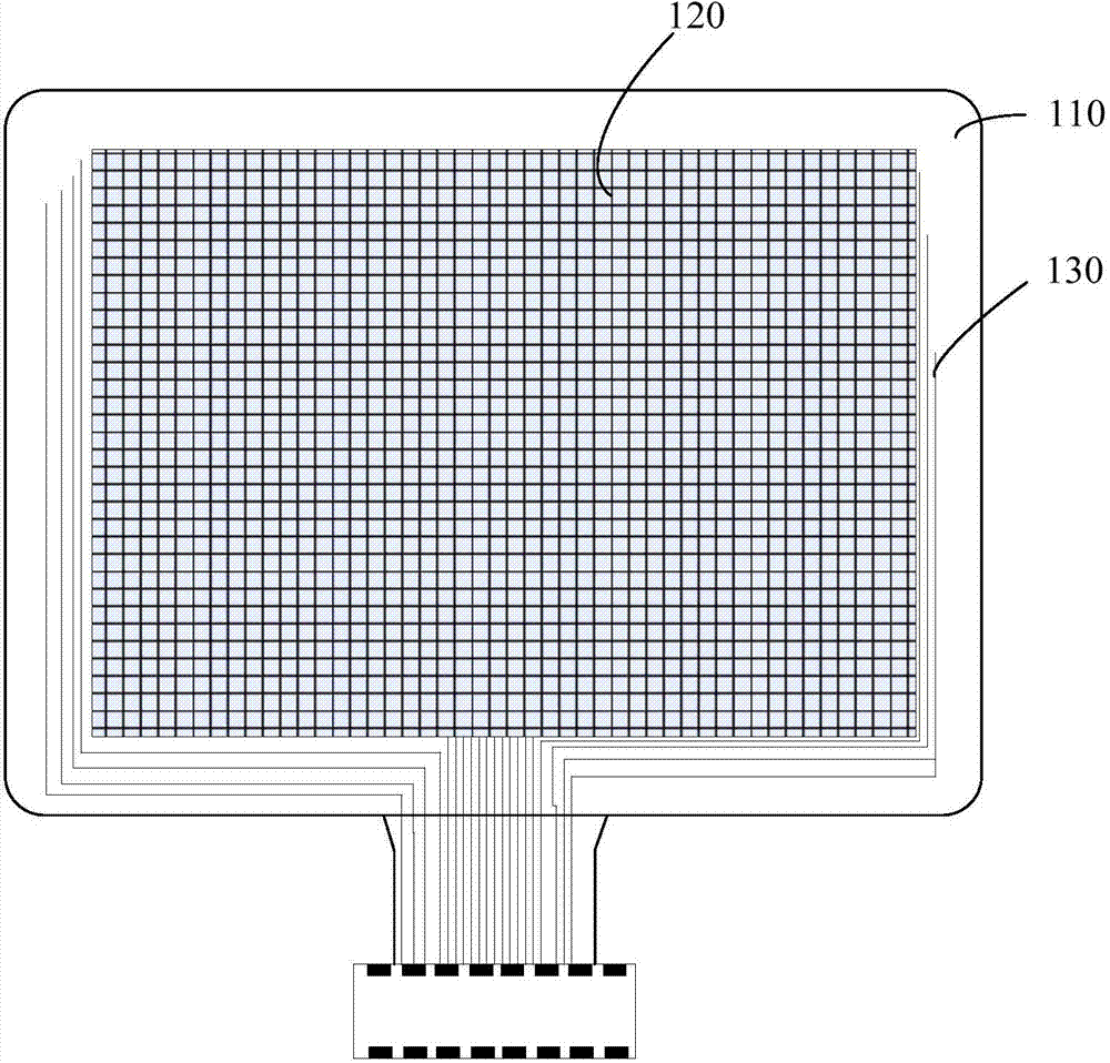
[0041] Please refer to figure 1 The capacitive biometric recognition sensor includes a base substrate 110, a conductive circuit 120 formed on the base substrate 110, and an electrode lead 130 connected to the conductive circuit 120.

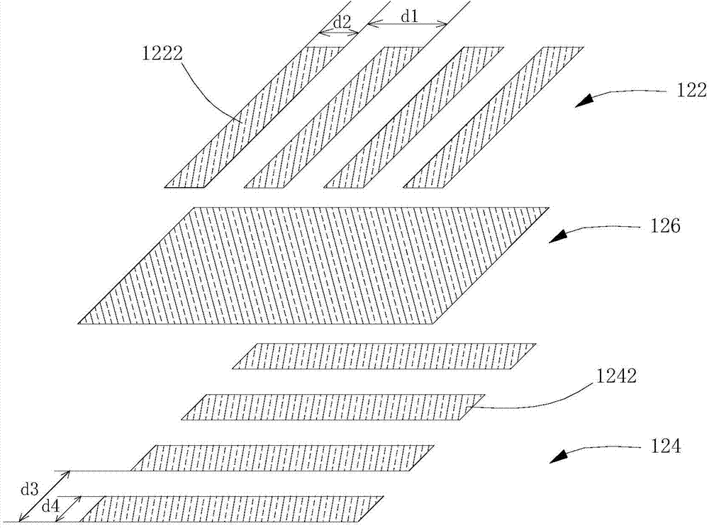
[0042] Please refer to figure 2 with image 3 The conductive circuit 120 includes an insulating layer 126 with a first conductive layer 122 and a second conductive layer 124 in between. In the present invention, the first conductive layer 122 is used as a sensing electrode, and the second conductive layer 124 is used as a driving electrode. However, it should be pointed out that the first conductive layer 122 and the second conductive layer 124 are not distinguished by themselves, and are specifically used as the kind of electrode. , Depends on the external chip.

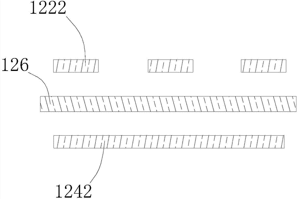
[0043] The first conductive layer 122 includes a plurality of first electrode lines 1222 insulated and distributed from each other. The second conductive layer 124 includes a plurality of...

Embodiment 2

[0064] Please refer to Picture 11 , The capacitive biometric recognition sensor includes a plurality of first electrode wires 210 for forming a first conductive layer, a first insulating substrate 220, an insulating layer 230, and a plurality of second electrode wires 240 for forming a second conductive layer And a second insulating substrate 250. The first electrode wire 210 is disposed on the first insulating substrate 220, the second electrode wire 240 is disposed on the second insulating substrate 250, and the insulating layer 230 separates the first electrode wire 210 from the second electrode wire 240. The material of the first insulating substrate 220 and the second insulating substrate 250 can be the same or different, and can be selected from PET (Polyethylene terephthalate), PMMA (Polymethyl Methacrylate, polymethyl methacrylate). Ester), PC (Polycarbonate, polycarbonate), COC (Cyclo Olefin Copolymers), COP (Cyclo Olefin Polymers, cyclic olefin copolymer) and other o...

Embodiment 3

[0066] Please refer to Picture 12 As an improvement of the second embodiment, in order to improve the adhesion performance between the first electrode line 210 and the first insulating substrate 220, and to improve the adhesion performance between the second electrode line 240 and the second insulating substrate 250, the first A first matching layer 260 is additionally provided between the electrode wires 210 and the first insulating substrate 220, and a second matching layer 270 is additionally provided between the second electrode wires 240 and the second insulating substrate 250. The material of the first electrode line 210 and the second electrode line 240 can be metal or a mixture of metal and organic resin with continuous electrical conductivity. The material of the first matching layer 260 and the second matching layer 270 can be ITO (oxidized Indium tin), the thickness is 10nm ~ 2μm.


PUM

PropertyMeasurementUnit
Areaaaaaaaaaaa
Diameteraaaaaaaaaa
Thicknessaaaaaaaaaa

Abstract

The invention relates to a capacitive biometric feature recognition sensor which comprises a first conductive layer, a second conductive layer and an insulating layer, wherein the first conductive layer includes a plurality of first electrode wires distributed in a mutually-isolated mode, the second conductive layer includes a plurality of second electrode wires distributed in a mutually-isolated mode, the projections of the second electrode wires on the plane where the first electrode wires are arranged intersect with the first electrode wires, and the insulating layer is arranged between the first conductive layer and the second conductive layer. According to the capacitive biometric feature recognition sensor, mutual-induction conductance is formed through the mutually-isolated first electrode wires and the mutually-isolated second electrode wires, whether a subcutaneous layer is in contact with mutual-induction conductance can be detected according to the change of capacitance, the CMOS semiconductor technology does not need to be adopted to form a fingerprint recognition sensor on a substrate, the problem of breakage due to pressing with great force does not occur, and the cost is reduced.

Description

Technical field [0001] The invention relates to the field of electronic sensing, in particular to a capacitive biometric identification sensor. Background technique [0002] The traditional fingerprint recognition sensor is formed on a single crystal silicon substrate, so there is a problem of cracking when the finger is pressed hard. In order to prevent the silicon chip from being easily damaged by the user's countless pressings or abnormal pressings, the existing solution generally uses high-hardness sapphire to protect the finger fingerprint sensor of the silicon substrate, but the cost of sapphire is high, resulting in the entire finger fingerprint identification system higher cost. [0003] The existing fingerprint silicon chip is formed by the CMOS semiconductor process to form a matrix fingerprint recognition sensor. The process is complicated, and the fingerprint imaging sensor with the silicon substrate as the substrate is prone to brittleness. Therefore, a protective len...

Claims


Application Information

Patent Timeline
IPC IPC(8): G06K9/00
Inventor 刘伟唐根初蒋芳
Owner NANCHANG VIRTUAL REALITY RES INST CO LTD
Why Eureka
Try Eureka