Laser cutting machine capable of improving splitting yield of LED chip

A technology of LED chip and laser cutting machine, applied in laser welding equipment, welding equipment, metal processing equipment, etc., can solve the problems of difficult cleaning, too deep cutting depth, and reducing the degree of sidewall ablation.

Active Publication Date: 2014-05-14
INNO LASER TECH CORP LTD +1
View PDF7 Cites 9 Cited by
  • Summary
  • Abstract
  • Description
  • Claims
  • Application Information

AI Technical Summary

Problems solved by technology

One is to use an ultrafast laser to form a cutting line inside the substrate to reduce the degree of ablation of the sidewall, but due to the high design cost, the equipment cost is high
Another way is to etch with high-temperature sulfuric acid / phosphoric acid after laser scribing to remove the ablation. Although the cost of this method is low, the steps are complicated, and the problem of etching is that it is not easy to clean when the cutting depth is too deep. Clean, but lack of depth and poor splitting yield
Especially in the existing laser cutting machines, the cutting is usually performed with the preset power laser emitted by the laser head, resulting in too deep or too shallow cutting depth. If it is too deep, the ablation area will be larger. If it is too shallow, the LED chips are not easy to split. Therefore, the above laser cutting method makes it difficult to improve the splitting yield of LED chips.

Method used


Image

  • Laser cutting machine capable of improving splitting yield of LED chip
  • Laser cutting machine capable of improving splitting yield of LED chip
  • Laser cutting machine capable of improving splitting yield of LED chip

Examples


Embodiment Construction

[0024] The present invention will be described in more detail below in conjunction with the accompanying drawings and embodiments.

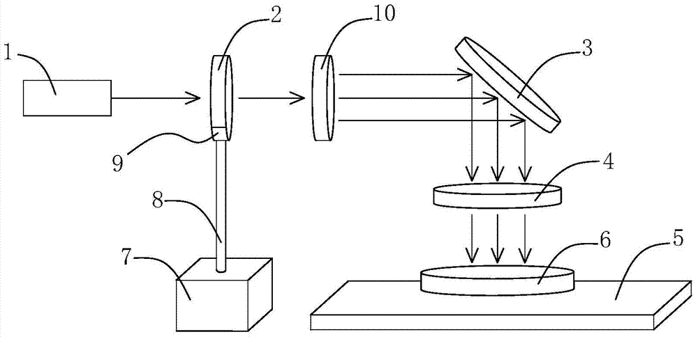
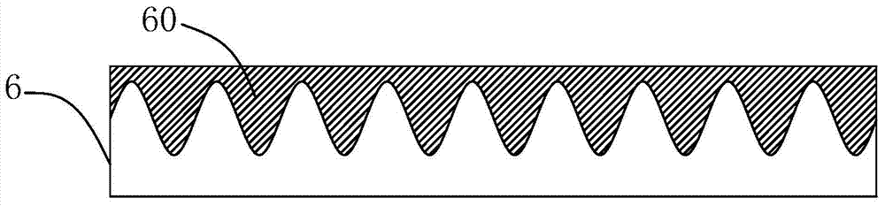
[0025] The invention discloses a laser cutting machine capable of improving the splitting yield of LED chips. Figure 1 to Figure 5 As shown, it includes a laser head 1 and a rotating mechanism 7, and along the laser transmission direction of the laser head 1, a 1 / 2 wave plate 2, a beam splitter 10, a reflector 3, a focusing mirror 4 and a moving stage 5, and an LED The chip 6 is placed on the mobile stage 5, and the 1 / 2 wave plate 2 is arranged on the rotating mechanism 7. As a preferred method, the power output end of the rotating mechanism 7 is provided with a drive rod 8, and the end of the drive rod 8 is provided with There is a hollow seat 9, and the 1 / 2 wave plate 2 is fixed on the hollow seat 9. The rotation mechanism 7 drives the 1 / 2 wave plate 2 to rotate around the radial direction of the 1 / 2 wave plate 2. In practical applications, th...


PUM

PropertyMeasurementUnit
Light source wavelengthaaaaaaaaaa

Abstract

The invention discloses a laser cutting machine capable of improving the splitting yield of an LED chip. The laser cutting machine comprises a laser head and a rotating mechanism. A 1 / 2 wave plate, s beam splitter mirror, a reflector, a focus lens and a movable carrying table are sequentially arranged in the laser transmission direction of the laser head. The LED chip is placed on the movable carrying table. The 1 / 2 wave plate is arranged at the power output end of the rotating mechanism. The rotating mechanism drives the 1 / 2 wave plate to rotate in the radial direction of the 1 / 2 wave plate. A laser beam which can form a periodic deep and shallow notch on the LED chip is generated under the rotation action of the 1 / 2 wave plate. The laser beam emitted by the 1 / 2 wave plate is split into at least two sub-laser-beams through the beam splitting mirror. The sub-laser-beams are transmitted to the LED chip sequentially through the reflector and the focus lens. The sub-laser-beams sequentially cut the same notch, the deep range and the shallow range of each nick are gradually increased, and therefore the LED chip can be more easily split off, the ablation area of the side wall of the LED chip is reduced after cutting is conducted, and the ablation degree of the side wall of a sapphire substrate is low.

Description

technical field [0001] The invention relates to a laser cutting machine, in particular to a laser cutting machine capable of improving the splitting yield of LED chips. Background technique [0002] The process of mechanical splitting after laser scribing is a common process in the LED chip cutting process, especially applied to blue LEDs based on sapphire. At present, blue LED chips based on sapphire are doped with phosphor and Capable of producing white light, this kind of LED will be the mainstream in the lighting field in the future. At the same time, how to further increase brightness and reduce costs has been a subject of the industry's efforts. After adopting laser scribing, although the grain separation technology of mechanical splitting has high production rate and low cost, the side wall of the sapphire substrate is ablated during laser scribing, such as Image 6 As shown, the laser emitted by the laser head 1 sequentially passes through the reflector 3 and the foc...

Claims


Application Information

Patent Timeline
IPC IPC(8): B23K26/064B23K26/38
CPCB23K26/064B23K26/067B23K26/38
Inventor 陈鸿隆
Owner INNO LASER TECH CORP LTD
Why Eureka
Try Eureka