High-frequency large-power silicon carbide MOSFET module

A silicon carbide, high-power technology, applied in electrical components, electrical solid devices, circuits, etc., can solve the power module power density is not high, the internal power loop parasitic inductance is large, and cannot meet the requirements of high power density and low parasitic inductance And other issues

Inactive Publication Date: 2014-05-14
嘉兴斯达微电子有限公司
View PDF4 Cites 9 Cited by
  • Summary
  • Abstract
  • Description
  • Claims
  • Application Information

AI Technical Summary

Problems solved by technology

[0006] At present, the most widely used power module package in the power electronics industry still adopts a package structure with a width of 34mm and 62mm. The module structure has a height of 30mm. The power density of this type of power module is not high, and the parasitic inductance of its internal power circuit is relatively large. , cannot meet the requirements of high power density and low parasitic inductance in some application fie

Method used


Image

  • High-frequency large-power silicon carbide MOSFET module
  • High-frequency large-power silicon carbide MOSFET module
  • High-frequency large-power silicon carbide MOSFET module

Examples


Embodiment

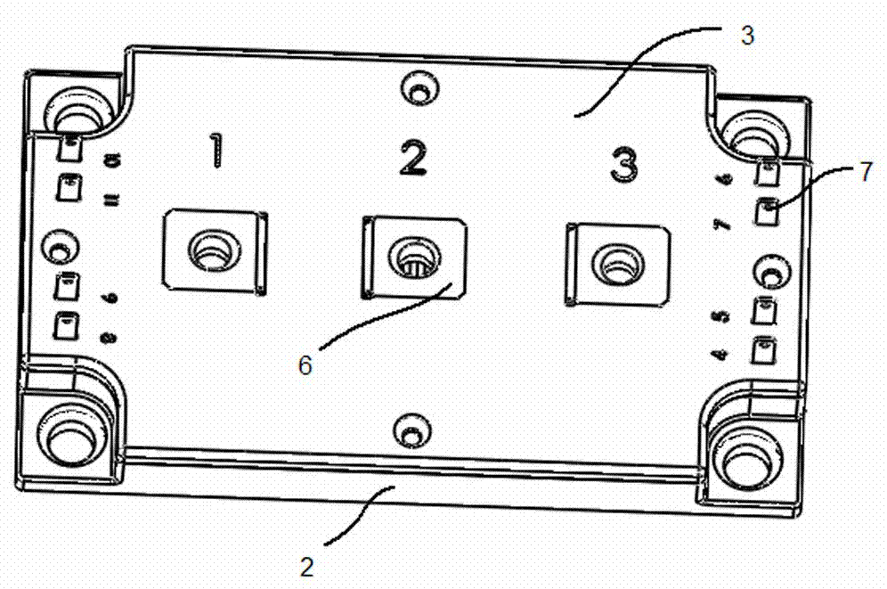
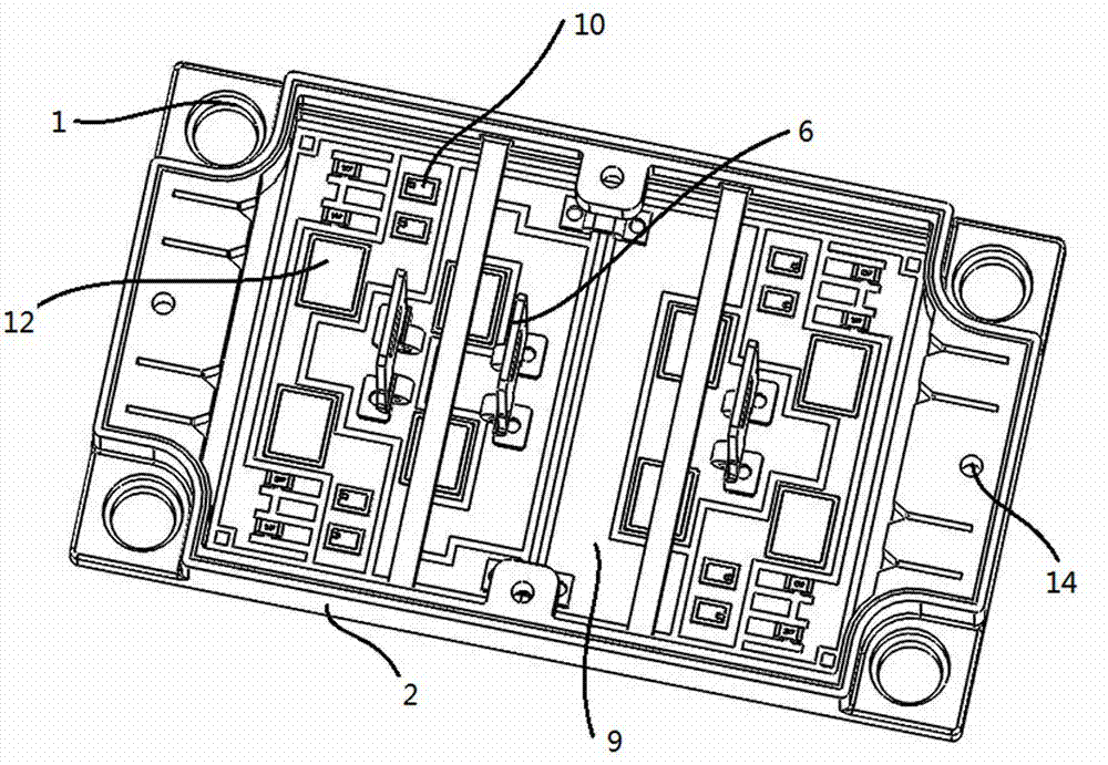
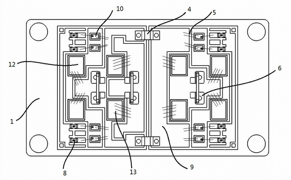
[0027] Embodiment: As shown in the figure, the present invention mainly includes: a heat dissipation substrate 1, a casing, and a circuit structure packaged in the casing; the casing includes a casing 2 and an outer cover 3 covering the casing, and the circuit structure includes power terminals 6. Signal terminal 7, insulating ceramic substrate 9, silicon carbide mosfet chip 10, silicon carbide SBD chip 12, 13;

[0028] The insulating ceramic substrate 9 is welded to the heat dissipation substrate 1 by high temperature reflow, and the silicon carbide mosfet chip 10 and the silicon carbide SBD chip 12, 13 are welded on the insulating ceramic substrate 9, and the silicon carbide mosfet chip 10 and the silicon carbide SBD chip 12, 13 are connected with the The circuit structure etched on the insulating ceramic substrate 9 is connected, and the silicon carbide mosfet chip 10 and the silicon carbide SBD chip 12, 13 are connected to each other through the aluminum wire 5, and at leas...


PUM


Abstract

Disclosed is a high-frequency large-power silicon carbide MOSFET module. The high-frequency large-power silicon carbide MOSFET module comprises a heat dissipation substrate, a shell and a circuit structure packaged into the shell. The shell comprises an outer shell and an outer cover covering the outer shell. The circuit structure comprises a power terminal, a signal terminal, an insulating ceramic substrate, a silicon carbide MOSFET chip and a silicon carbide SBD chip. The insulating ceramic substrate is welded to the heat dissipation substrate through high-temperature reflow soldering, and the silicon carbide MOSFET chip and the silicon carbide SBD chip are welded to the insulating ceramic substrate, connected with the circuit structure etched on the insulating ceramic substrate and connected with each other through an aluminum wire. At least three power terminals are welded to corresponding positions of the insulating ceramic substrate. The high-frequency large-power silicon carbide MOSFET module can be applied to the application field with the switching frequency larger than 500 kHz and the output power larger than 100 kW.

Description

technical field [0001] The invention relates to a high-frequency and high-power silicon carbide MOSFET module, which belongs to the technical field of semiconductor module packaging. technical background [0002] High-frequency high-power semiconductor modules are mainly used in applications of electric energy conversion, such as: induction heating, inverter welding machines, UPS, electrolytic plating power supplies, etc. Traditional high-power semiconductor modules mainly include: IGBT (insulated gate bipolar transistor), Power MOSFET (field effect transistor), thyristor and power diode, etc., power semiconductor module is to package the above power semiconductor chips into various basic circuit units, which are applied to the power circuit of power electronic system. [0003] At present, for the application of high-power device switching frequency up to 100kHz, silicon-based high-voltage mosfet devices or silicon-based coolmos devices are generally used, while traditional ...

Claims


Application Information

Patent Timeline
IPC IPC(8): H01L23/36H01L23/492H01L23/04
CPCH01L2924/0002
Inventor 刘志宏
Owner 嘉兴斯达微电子有限公司
Why Eureka
Try Eureka