Small beam-switchable antenna capable of conducting omni-directional scanning in H face perpendicular to antenna plane

A technology for scanning beams and antennas, applied in the field of electronics, can solve the problems of inability to achieve full coverage of the antenna, narrow beams, and reduce the size of the antenna, and achieve the effect of good application value, compact antenna structure, and expansion of the application range.

Inactive Publication Date: 2014-05-14
UNIV OF ELECTRONICS SCI & TECH OF CHINA
View PDF5 Cites 8 Cited by
  • Summary
  • Abstract
  • Description
  • Claims
  • Application Information

AI Technical Summary

Problems solved by technology

By switching the switch state connecting the central circular feed patch and the fan-shaped metal patch to make different element antennas work, so the antenna can realize beam switching in five directions in the plane where the antenna is located. However, due to the radiator of the antenna Due to the limitation of characteristics, the beam of the antenna on the E plane (parallel to the direction of the electric field) is relatively narrow, and the 3dB lobe width of each beam on the plane where the antenna is located is 45°. By switching these five beams, each adjacent two beams There is a gap of about 27°

Method used


Image

  • Small beam-switchable antenna capable of conducting omni-directional scanning in H face perpendicular to antenna plane
  • Small beam-switchable antenna capable of conducting omni-directional scanning in H face perpendicular to antenna plane
  • Small beam-switchable antenna capable of conducting omni-directional scanning in H face perpendicular to antenna plane

Examples


Embodiment Construction

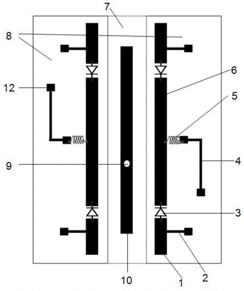
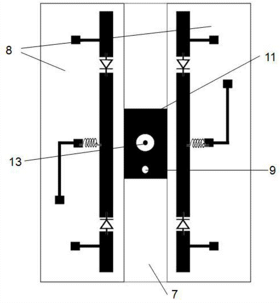
[0024] The present invention is described in an embodiment in which the frequency band of scanning mode 1 is 5.2-5.4G, and the frequency band of scanning mode 2 is 4.4-4.8G.

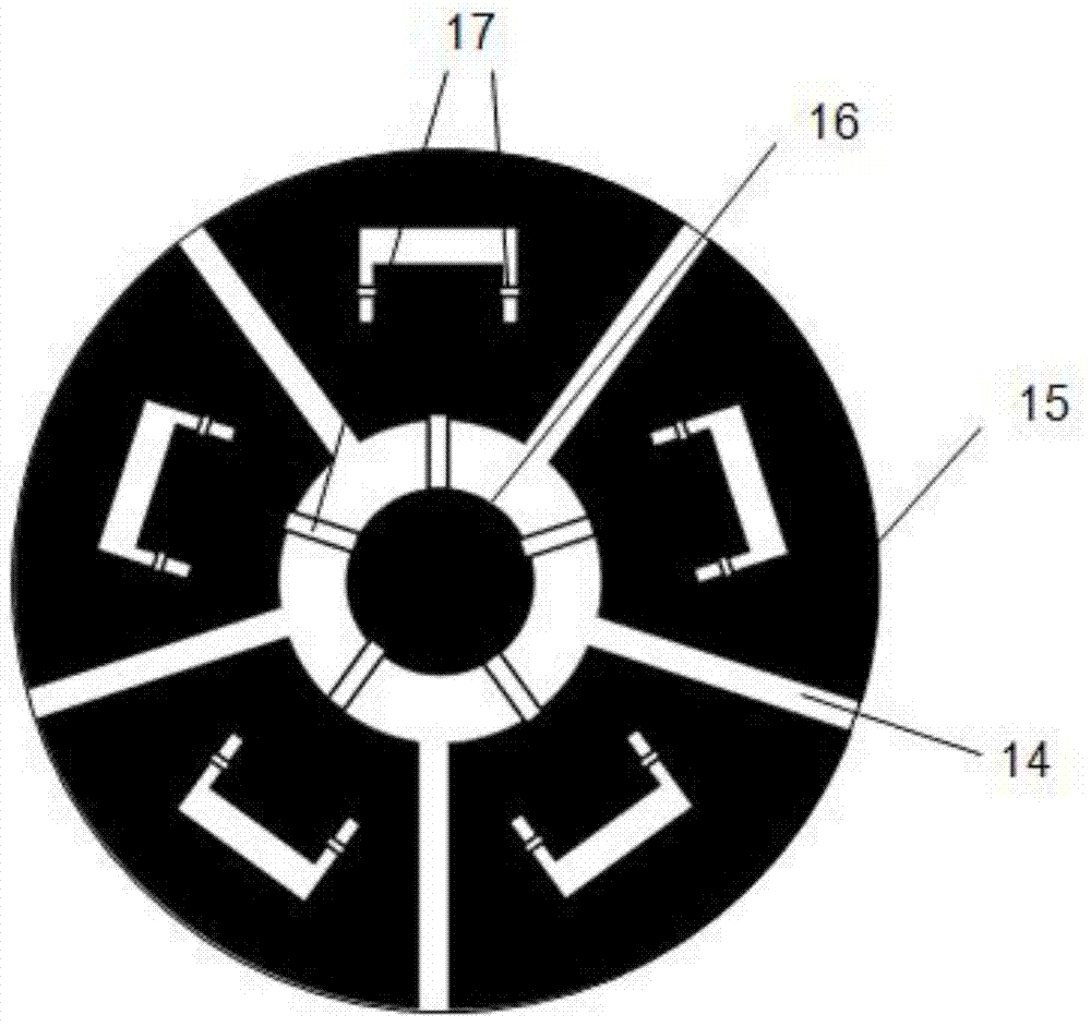
[0025] The structure of the antenna is as Figure 2-Figure 4 As shown, it includes: a rectangular middle insulating substrate 7 with a feed input port, a chip vibrator 10 arranged on its upper surface, a metal ground plate 11 arranged on its lower surface, and four quadrilaterals that are closely attached to the upper and lower surfaces of the middle insulating substrate 7. Block rectangular surface layer insulation substrate 8 and the parasitic patch that is arranged on its surface, PIN diode switch 3, the bias circuit of control switch. SMD vibrator 10, parasitic patch, metal ground plate 11, first high impedance line 4, second high impedance line 2 and metal patch 12 are all copper foils with a thickness of 0.07mm; middle insulating substrate 7, surface insulating substrate 8 The relative dielectric ...


PUM


Abstract

The invention provides a small beam-switchable antenna capable of conducting omni-directional scanning in an H face perpendicular to an antenna plane, belongs to the technical field of electronics, and particularly relates to a beam-switchable antenna technology with PIN diode switches. The antenna comprises a rectangular middle layer insulating substrate with a feed input port, patch vibrators arranged on the surface of the middle layer insulating substrate, a metal grounding plate arranged on the lower surface of the middle layer insulating substrate, four rectangular surface layer insulating substrates tightly attached to the upper surface and the lower surface of the middle layer insulating substrate, parasitic patches, the PIN diode switches and biasing circuits of control switches, wherein the parasitic patches, the PIN diode switches and the biasing circuits are arranged on the surfaces of the surface layer insulating substrates. Eight beam radiation directions are switches by controlling switching on and switching off of the control switches, and therefore omni-directional scanning in the vertical plane is achieved, the scanning dimension of the antenna is expanded to the plane perpendicular to the antenna from the plane where the antenna is located, the rough scanning method and the fine scanning method are achieved under two different working frequency bands, the application range of the antenna is widened, and different environment requirements can be met.

Description

technical field [0001] The invention belongs to the field of electronic technology, in particular to the beam switchable antenna technology with a PIN diode switch. Background technique [0002] As more and more information content needs to be transmitted, modern communication systems have higher and higher requirements on the information transmission rate in wireless communication, but due to the existence of multipath fading, the data transmission rate decreases with the increase of signal transmission distance . Numerous studies have shown that the proper use of antennas with switchable beams is one way to solve this problem. The pattern reconfigurable antenna can change the pattern of the transmitting and receiving antennas in real time according to changes in the communication environment, thereby effectively reducing noise interference, combating multipath fading, and improving the information transmission rate. [0003] Literature "A circular disc-shaped antenna wit...

Claims


Application Information

Patent Timeline
IPC IPC(8): H01Q9/04H01Q3/24
Inventor 王任王秉中丁霄
Owner UNIV OF ELECTRONICS SCI & TECH OF CHINA
Why Eureka
Try Eureka