
Voltage regulating device

A technology of voltage adjustment circuit and feedback voltage, which is applied in the direction of adjusting electrical variables, control/regulation systems, instruments, etc., can solve the problems of large area, large device area, and small capacitance value per unit area, so as to reduce the circuit area and chip Effects of cost and area reduction

Active Publication Date: 2014-05-21
SHANGHAI HUAHONG GRACE SEMICON MFG CORP
View PDF5 Cites 6 Cited by
  • Summary
  • Abstract
  • Description
  • Claims
  • Application Information

AI Technical Summary

Problems solved by technology

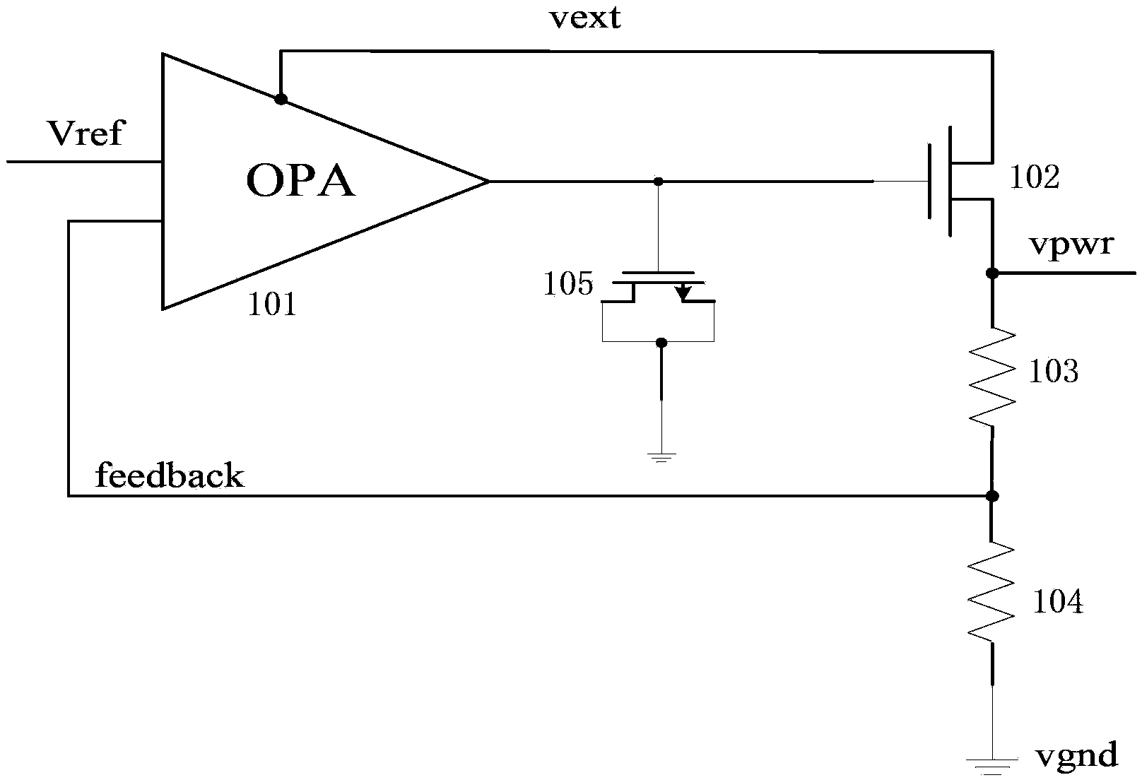
[0007] The withstand voltage capability of the second MOS transistor 105 is greater than the reference voltage output by the voltage adjustment circuit. When the reference voltage output by the voltage adjustment circuit is a high voltage such as a voltage above 3.3V, the gate of the second MOS transistor 105 must also be able to withstand high voltage. , so that the second MOS transistor 105 must use a high-voltage device, and for a high-voltage device to withstand high voltage, the thickness of the gate oxide layer must be increased, and a thicker gate oxide layer will cause the capacitance per unit area of ​​the device to be very small, so when the required compensation When the capacitance value is the same, the area of ​​the high-voltage device must be increased after the thickness of the gate oxide layer is increased to keep the supplementary capacitance constant, which will result in a large area of ​​the device
In some cases, the capacitor area of ​​the second MOS transistor 105 may be larger than the VR circuit area itself

Method used


Image

  • Voltage regulating device
  • Voltage regulating device

Examples


Embodiment Construction

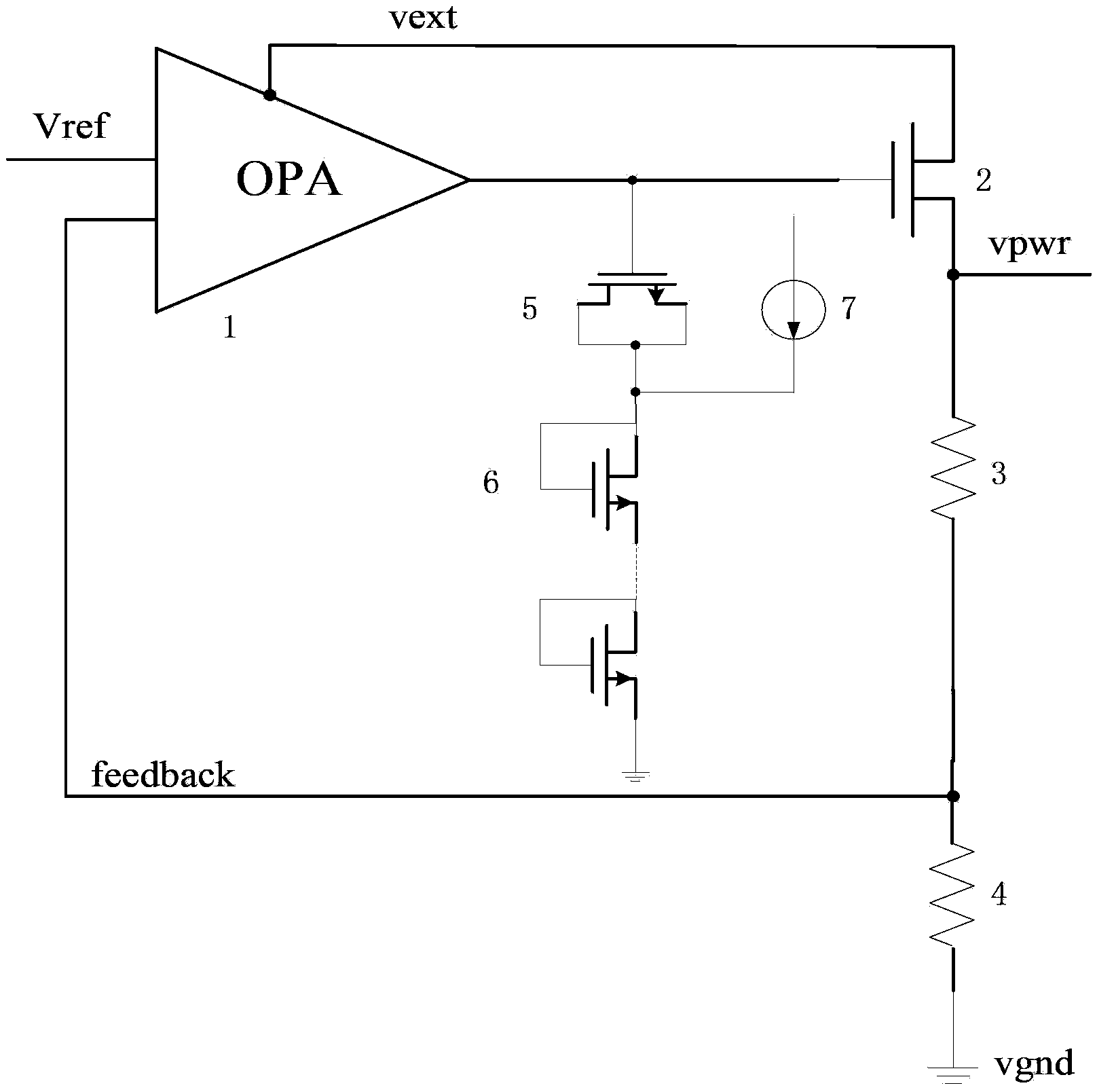
[0023] Such as figure 2 Shown is a schematic structural diagram of the voltage adjustment circuit of the embodiment of the present invention. The voltage adjustment circuit according to the embodiment of the present invention includes:

[0024] An operational amplifier 1, one input terminal of the operational amplifier 1 is connected to a reference voltage Vref, the other input terminal is connected to a feedback voltage feedback, and the operating power supply of the operational amplifier 1 is an external voltage vext.

[0025] A first NMOS drive tube 2, the source of the first NMOS drive tube 2 is used as the output terminal of the output voltage vpwr of the voltage adjustment circuit, and the drain of the first NMOS drive tube 2 is connected to the external voltage vext; The gate of the first NMOS drive transistor 2 is connected to the output terminal of the operational amplifier 1 .

[0026] A first resistor 3 and a second resistor 4 are connected in series between the ...


PUM


Abstract

The invention discloses a voltage regulating device. A third MOS (metal oxide semiconductor) transistor is serially connected between a ground and a source of a second MOS transistor as a compensation capacitor to form a diode structure, the current is provided for a serial connecting structure through a current source, and the serial connecting structure can provide a fixed voltage for a source and a drain of the second MOS transistor. The voltage regulating device has the advantages that the fixed voltage can be used for reducing the voltage of the second MOS transistor during actual working; when the output voltage of the voltage regulating circuit is the high voltage, the voltages of a grid, the source and the drain of the second MOS transistor can maintain the low voltage, so the second MOS transistor can adopt low-voltage devices, the required thickness of a grid oxidizing layer of the second MOS transistor is greatly reduced, and meanwhile, the capacitance of the unit area of the second MOS transistor is increased; under the condition of not changing the required compensation capacitor value, the area of the second MOS transistor is greatly reduced, so the area of the circuit is reduced, and the cost of a chip is reduced.

Description

technical field [0001] The present invention relates to a semiconductor integrated circuit, in particular to a voltage regulation circuit (VR). Background technique [0002] Such as figure 1 As shown, it is a schematic structural diagram of an existing voltage adjustment circuit, and the existing voltage adjustment circuit includes: [0003] An operational amplifier 101, one input terminal of the operational amplifier 101 is connected to the reference voltage Vref, and the other input terminal is connected to the feedback voltage feedback, and the operating power supply of the operational amplifier 101 is an external voltage vext. [0004] A first NMOS drive tube 102, the source of the first NMOS drive tube 102 is used as the output terminal of the reference voltage vpwr, and the drain of the first NMOS drive tube 102 is connected to the external voltage vext; the first NMOS drive tube The gate of 102 is connected to the output terminal of the operational amplifier 101 . ...

Claims


Application Information

Patent Timeline
Patent Type & Authority Applications(China)
IPC IPC(8): G05F1/56
Inventor 唐成伟
Owner SHANGHAI HUAHONG GRACE SEMICON MFG CORP
Learn More