Fully press-fit packaged high-voltage semiconductor devices

A semiconductor and high-voltage technology, which is applied in the field of high-voltage semiconductor devices with full crimping packaging, can solve the problem that the chip reliability cannot meet the high-voltage products and high-current products, etc. Effect

Active Publication Date: 2017-08-29
HUBEI TECH SEMICON
View PDF1 Cites 0 Cited by
  • Summary
  • Abstract
  • Description
  • Claims
  • Application Information

AI Technical Summary

Problems solved by technology

[0002] The traditional chip manufacturing of semiconductor devices is made by welding chips and electrode sheets through solder at high temperature, and there are welding stress and welding voids. When the voltage reaches 5000V or more, the deformation stress of the high-temperature soldered chip makes the reliability unable to meet the requirements of high-voltage products and high-current products. It is urgent to adopt new semiconductor device structures and new semiconductor process technologies to meet new requirements.

Method used


Image

  • Fully press-fit packaged high-voltage semiconductor devices
  • Fully press-fit packaged high-voltage semiconductor devices
  • Fully press-fit packaged high-voltage semiconductor devices

Examples


Embodiment Construction

[0024] Combine below Figure 1 to Figure 5 The present invention is further described.

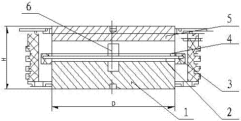
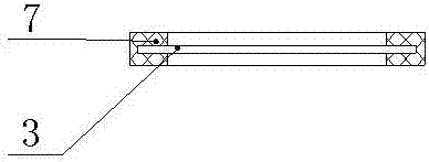
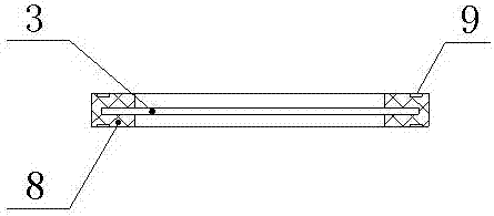
[0025] Such as figure 1 shown. High-voltage semiconductor devices are fully crimped and packaged, and the lower sealing part 1 of the tube case, the lower molybdenum wafer 2, the semiconductor chip 3, the upper molybdenum wafer 4, the gate lead assembly 6, and the upper sealing part 5 of the tube case are packaged by cold pressure made. Install the gate lead assembly 6 in the center opening of the upper sealing part 5 of the tube case, the gate lead assembly 6 is higher than the surface of the upper sealing part 5 of the tube case, and snap into the center through hole of the upper molybdenum disc 4, and position the upper molybdenum disc . The diameter D of the device table is: 23mm≤D≤140mm, and the thickness H of the tube shell is: 23mm≤H≤40mm. The internal semiconductor chip 3 of the device and the upper and lower molybdenum wafers 2, 4 and the upper and lower sealing parts 1, 5 of...


PUM


Abstract

The invention relates to a full-crimping packaging high voltage semiconductor device, belongs to the high voltage semiconductor device technology field and mainly solves problems of welding stress and a welding cavity existing in high temperature welding of a chip and an electrode sheet through a welding material in the prior art. The full-crimping packaging high voltage semiconductor device is mainly characterized in that a tube casing lower sealing member, a lower molybdenum disk, a semiconductor chip, an upper molybdenum disk, a gate pole leading wire assembly and a tube casing upper sealing member are in crimping contact sequentially, the center of the tube casing upper sealing member is provided with a mounting hole, the center of the upper molybdenum disk is provided with a positioning hole, and the gate pole leading wire assembly is clamped in the positioning hole. The full-crimping packaging high voltage semiconductor device can eliminate deformation and stress generated during high temperature welding of the chip, can satisfy characteristic requirements of the high voltage semiconductor device with the voltage greater than 5000V or a diameter of the chip greater than 4 inches, and is mainly applied to a high voltage soft start power source, a high voltage stationary reactive compensation power source, a high voltage pulse power power source and high voltage semiconductor devices in the field of high voltage DC power transmission.

Description

technical field [0001] The invention relates to a high-voltage semiconductor device, specifically a high-voltage semiconductor device in a fully crimped package, which is mainly used in the fields of high-voltage soft-start power supply, high-voltage static reactive compensation power supply, high-voltage pulse power supply, high-voltage direct current transmission and the like. Background technique [0002] The traditional chip manufacturing of semiconductor devices is made by welding chips and electrode sheets through solder at high temperature, and there are welding stress and welding voids. When the voltage reaches 5000V or more, the deformation stress of the high-temperature soldered chip makes the reliability unable to meet the requirements of high-voltage products and high-current products. It is urgent to adopt new semiconductor device structures and new semiconductor process technologies to meet new requirements. Contents of the invention [0003] Aiming at the ab...

Claims


Application Information

Patent Timeline
Patent Type & Authority Patents(China)
IPC IPC(8): H01L23/04H01L23/28H01L23/31H01L29/04
Inventor 刘鹏张桥颜家圣吴拥军孙亚男杨宁林煜风张明辉李娴任丽刘小俐
Owner HUBEI TECH SEMICON
Why Eureka
Try Eureka