Nonvolatile memory

A non-volatile, memory technology, applied in the field of memory, can solve the problems affecting the performance of resistive memory, etc., and achieve the effect of good rectification effect and high reading discrimination.

Inactive Publication Date: 2014-05-21
WINBOND ELECTRONICS CORP
View PDF9 Cites 0 Cited by
  • Summary
  • Abstract
  • Description
  • Claims
  • Application Information

AI Technical Summary

Problems solved by technology

However, the resistive memory with such a 1D1R structure often can only withstand one transition operation between the high resistance and low resistance states, thus affecting the performance of the resistive memory

Method used


Image

  • Nonvolatile memory
  • Nonvolatile memory
  • Nonvolatile memory

Examples


no. 1 example

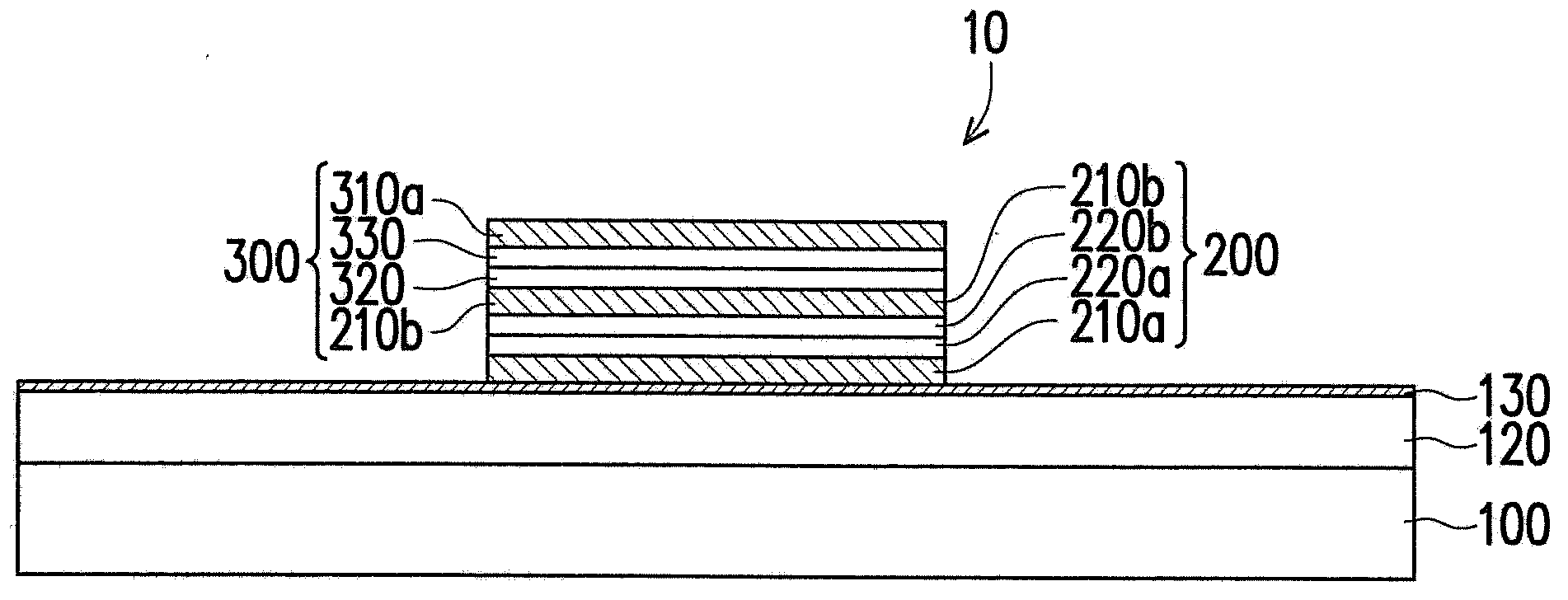
[0039] figure 1 is a schematic cross-sectional view of the nonvolatile memory according to the first embodiment of the present invention. Please refer to figure 1 , the nonvolatile memory 10 includes a unipolar resistive memory unit 200 and a diode unit 300 . The unipolar resistive memory cell 200 is disposed on the substrate 100 . The substrate 100 is, for example, a silicon substrate. In addition, the dielectric layer 120 is disposed between the unipolar resistive memory unit 200 and the substrate 100 . The material of the dielectric layer 120 is, for example, oxide, and its thickness is, for example, between 10 nm and 500 nm. The dielectric layer 120 is used to electrically isolate the unipolar resistive memory cell 200 from the substrate 100 . In addition, the adhesion layer 130 is selectively disposed between the unipolar resistive memory unit 200 and the dielectric layer 120 . The material of the adhesion layer 130 is, for example, titanium, and its thickness is, f...

no. 2 example

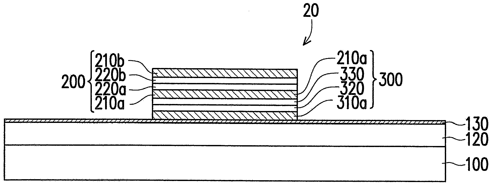
[0046] figure 2 is a schematic cross-sectional view of the nonvolatile memory according to the second embodiment of the present invention. Please refer to figure 2 The difference between the nonvolatile memory 20 and the nonvolatile memory 10 is that in the nonvolatile memory 20, the diode unit 300 is disposed on the adhesion layer 130, while the unipolar resistive memory unit 200 is disposed on the diode unit 300, and both share the electrode 210a.

no. 3 example

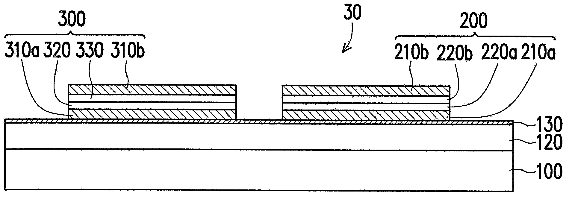
[0048] image 3 is a schematic cross-sectional view of the non-volatile memory according to the third embodiment of the present invention. Please refer to image 3, the difference between the nonvolatile memory 30 and the nonvolatile memory 10 is that: in the nonvolatile memory 30, the diode unit 300 and the unipolar resistive memory unit 200 are both arranged on the adhesion layer 130, and the diode unit The 300 and the unipolar resistive memory cell 200 are electrically connected to each other, for example, through interconnection lines (not shown). In this embodiment, the unipolar resistive memory cell 200 and the diode unit 300 each have a pair of electrodes, that is, the unipolar resistive memory cell 200 has an electrode 210a and an electrode 210b, and the diode unit 300 has an electrode 310a and an electrode 310b . In the unipolar resistive memory cell 200 , the electrode 210 a , the transition layer 220 a , the transition layer 220 b and the electrode 210 b are sequ...


PUM


Abstract

The invention discloses a nonvolatile memory comprising a unipolar resistive memory unit and a diode unit which are electrically connected. The diode unit comprises a first electrode, a second electrode, a cobalt oxide layer, and an indium zinc oxide layer. The first electrode and the second electrode are configured oppositely. The cobalt oxide layer is configured between the first electrode and the second electrode. The indium zinc oxide layer is configured between the first electrode and the cobalt oxide layer. The nonvolatile memory not only has a good rectification effect, but also may bear more than 100 times of converting operation between high resistance and low resistance and maintain high reading identification degree between the high resistance and the low resistance.

Description

technical field [0001] The present invention relates to a memory, and in particular to a non-volatile memory. Background technique [0002] Memory, as the name implies, is a semiconductor device used to store data or data. When the functions of computer microprocessors become stronger and stronger, and the programs and calculations performed by software become larger and larger, the demand for memory becomes higher and higher. In order to make large-capacity and cheap memory to meet the trend of this demand , Memory technology and process have become the driving force for semiconductor technology to continue to challenge high integration. Among all kinds of non-volatile memories, resistive memories have the advantages of low operating voltage, multi-state storage, long storage time, small area and simple structure, so resistive memories have become the trend of future memory development. [0003] Resistive memory generally includes resistive memory cells and diode cells. ...

Claims


Application Information

Patent Timeline
Patent Type & Authority Applications(China)
IPC IPC(8): H01L45/00H01L27/24
CPCH01L29/24H01L29/66969H01L29/8613H01L21/02425H01L21/02565H01L21/02631H10B63/84H10B63/20
Inventor 曾俊元李岱萤蔡宗霖
Owner WINBOND ELECTRONICS CORP
Why Eureka
Try Eureka