Low-temperature polycrystalline silicon thin film transistor, array substrate and manufacturing method of array substrate

A thin-film transistor and low-temperature polysilicon technology, which is applied in the direction of transistors, semiconductor/solid-state device manufacturing, and electric solid-state devices, can solve the problems of low-temperature polysilicon manufacturing process, low yield rate, and poor performance of thin-film transistors. Effects of defects and defects, performance improvement, and manufacturing process simplification

Active Publication Date: 2014-06-04
BOE TECH GRP CO LTD
View PDF3 Cites 20 Cited by
  • Summary
  • Abstract
  • Description
  • Claims
  • Application Information

AI Technical Summary

Problems solved by technology

[0004] It can be seen that the polysilicon and the source doped layer and drain doped layer are completed in two process flows, and the manufacturing process flow of low temperature polysilicon is not simple enough.
In addition, the ion implantation method to form the source doped layer region and the drain doped layer region will cause related defects and undesirable phenomena of the thin film transistor, the performance of the thin film transistor is poor, and the yield rate is low

Method used


Image

  • Low-temperature polycrystalline silicon thin film transistor, array substrate and manufacturing method of array substrate
  • Low-temperature polycrystalline silicon thin film transistor, array substrate and manufacturing method of array substrate
  • Low-temperature polycrystalline silicon thin film transistor, array substrate and manufacturing method of array substrate

Examples


Embodiment Construction

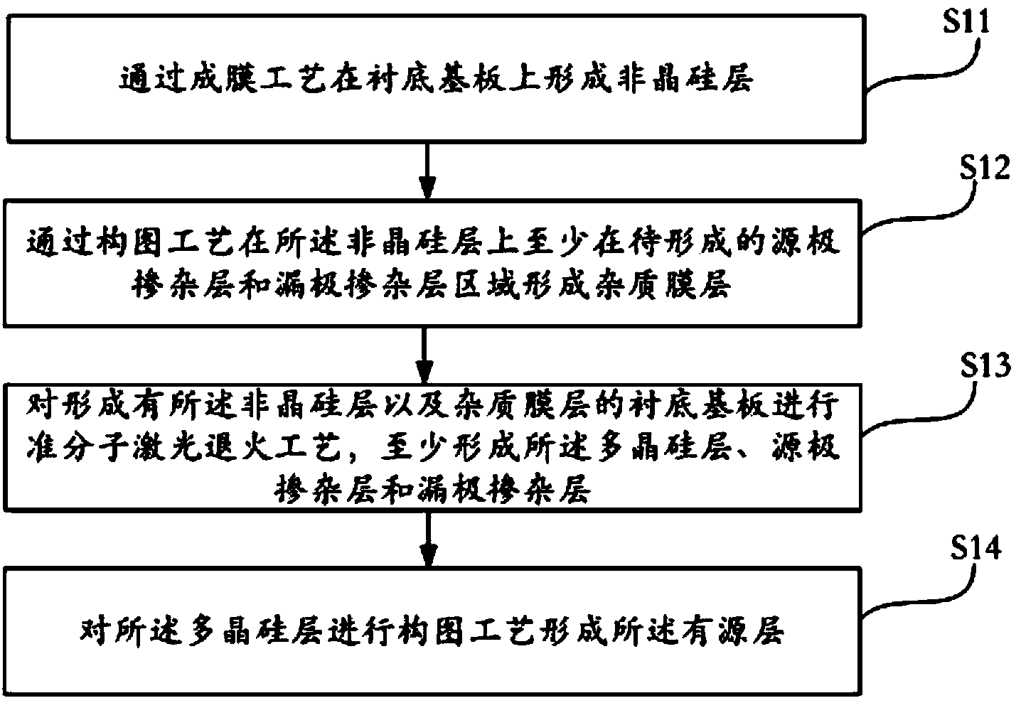
[0044] Embodiments of the present invention provide a low-temperature polysilicon thin film transistor, an array substrate and a manufacturing method thereof, which are used to simplify the manufacturing process of the thin film transistor and improve the performance of the thin film transistor.

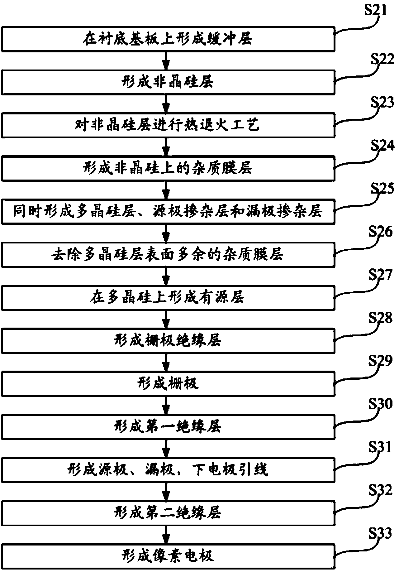
[0045] In the manufacturing method of the low-temperature polysilicon thin film transistor provided by the embodiment of the present invention, the source doped layer and the drain doped layer are simultaneously formed during the process of forming the polysilicon layer from the amorphous silicon layer, which simplifies the manufacturing process. The source doped layer and the drain doped layer are realized by doping in the polysilicon layer. In the present invention, the formation of doping ions in the polysilicon layer is achieved through excimer laser annealing, which avoids related defects and bad phenomena of thin film transistors caused by ion implantation, and improves the perf...


PUM


Abstract

The invention discloses a low-temperature polycrystalline silicon thin film transistor, an array substrate and a manufacturing method of the array substrate, so that manufacturing process procedures of the thin film transistor are simplified. The method includes the process that an active layer, a source electrode doping layer and a drain electrode doping layer are formed on a substrate, wherein the process that the active layer, the source electrode doping layer and the drain electrode doping layer are formed on the substrate includes the steps of forming an amorphous silicon layer on the substrate through a film forming technology, forming impurity film layers on at least a source electrode doping layer to be formed and a drain electrode doping layer to be formed on the amorphous silicon layer through a composition process, carrying out the excimer laser annealing process on the substrate provided with the amorphous silicon layer and the impurity film layers to at least form the polycrystalline silicon layer, the source electrode doping layer and the drain electrode doping layer, and the composition process is carried out on the polycrystalline silicon layer to form the active layer.

Description

technical field [0001] The invention relates to the field of manufacturing thin film transistors, in particular to a low-temperature polysilicon thin film transistor array substrate and a manufacturing method thereof. Background technique [0002] In pixel units of various display devices, a thin film transistor (Thin Film Transistor, TFT) that drives the display device by applying a driving voltage is widely used. Amorphous silicon (a-Si) materials with better stability and processability have been used in the active layer of TFTs, but the carrier mobility of a-Si materials is low, which cannot meet the needs of large-scale, high-resolution display devices requirements, especially the requirements of the next generation of active matrix organic light emitting display devices (Active Matrix Organic Light Emitting Device, AMOLED). Compared with amorphous silicon (a-Si) thin film transistors, polysilicon, especially low-temperature polysilicon thin film transistors, have high...

Claims


Application Information

Patent Timeline
Patent Type & Authority Applications(China)
IPC IPC(8): H01L21/336H01L21/84H01L29/786H01L29/08H01L27/12
CPCH01L27/1222H01L27/1285H01L29/0847H01L29/66757H01L29/78675H01L29/78618H01L27/1255H01L21/268H01L21/02422H01L21/02488H01L21/02532H01L21/02592H01L21/0262H01L21/02686H01L21/2254H01L28/60H01L21/02667H01L27/1274H01L29/66969
Inventor 毛雪
Owner BOE TECH GRP CO LTD
Why Eureka
Try Eureka