Structure and manufacturing method of power device MPT-TI-IGBT

A technology of -MPT-TI-IGBT and power device, which is applied to the structure and preparation field of power device-MPT-TI-IGBT, and can solve the problems of large on-state loss, very poor, and high saturation voltage drop V.

Inactive Publication Date: 2014-06-04
INST OF MICROELECTRONICS CHINESE ACAD OF SCI +2
View PDF4 Cites 4 Cited by
  • Summary
  • Abstract
  • Description
  • Claims
  • Application Information

AI Technical Summary

Problems solved by technology

The impurity concentration distribution corresponding to this electric field distribution is a very poor distribution, which means that the on-state resistance is quite large in the on-state, and the saturation voltage drop V of the device CE High, large on-state loss

Method used


Image

  • Structure and manufacturing method of power device MPT-TI-IGBT
  • Structure and manufacturing method of power device MPT-TI-IGBT
  • Structure and manufacturing method of power device MPT-TI-IGBT

Examples


Embodiment 1

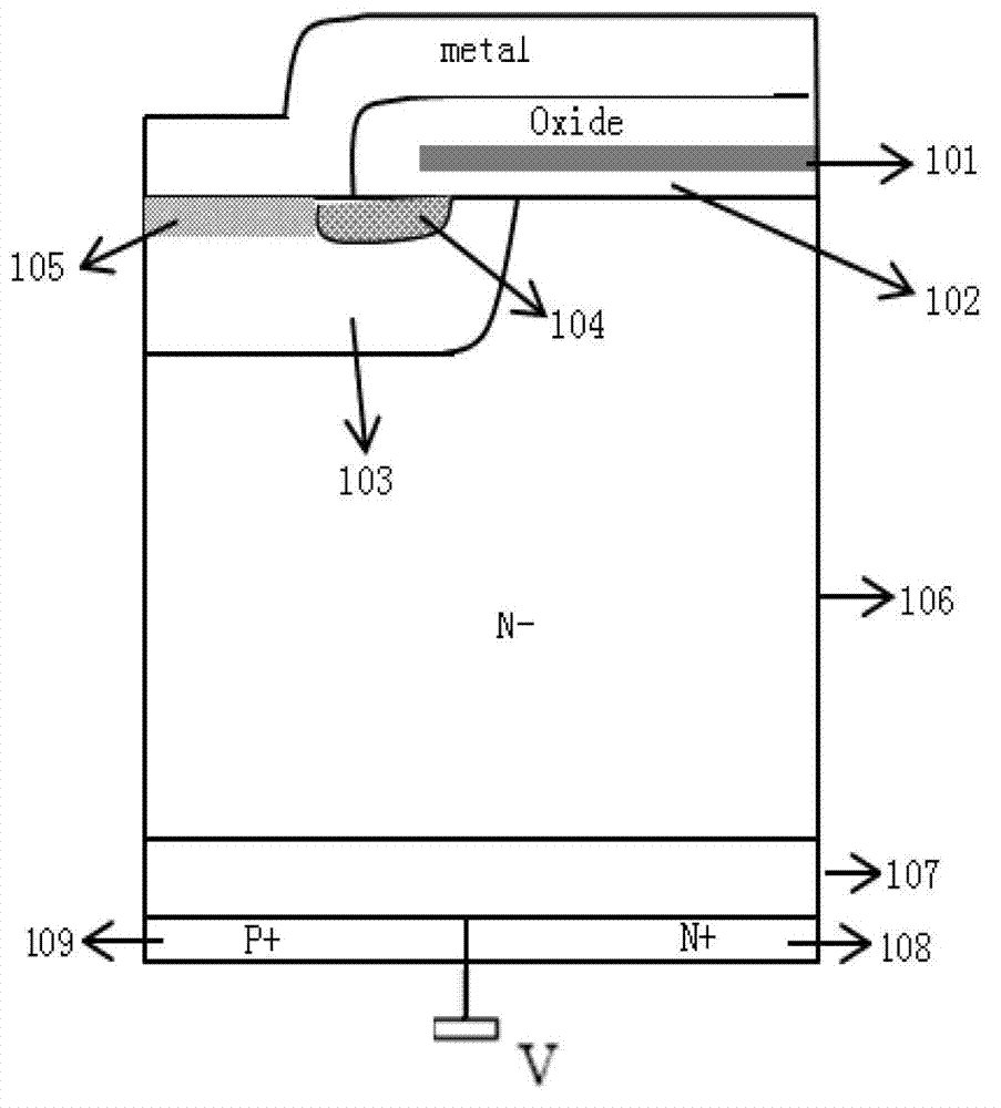
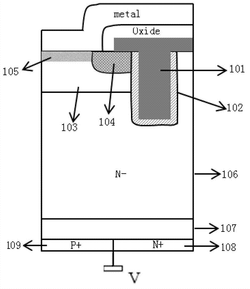
[0030] After the front side process is completed, the silicon wafer is thinned from the back side, and a micro-through layer 107 is formed under the drift region 106;

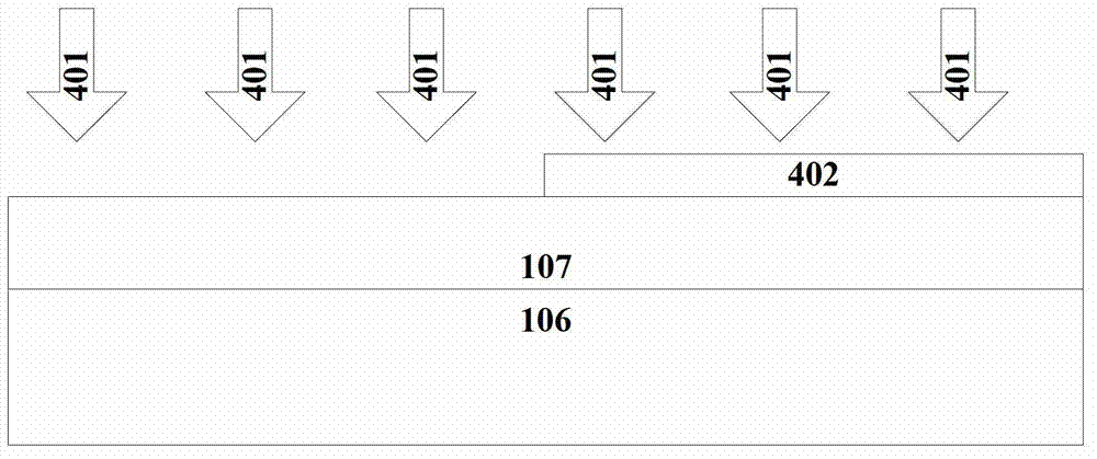
[0031] see image 3 , using a mask to define the shape of the photoresist 402 and injecting N-type doping (or P-type doping) 401;

[0032] see Figure 4 , forming a short circuit region 108 (or collector region 109 ) of the first (or second) conductivity type after degelling and annealing;

[0033] see Figure 5 , using a mask to define the shape of the photoresist 404 and injecting P-type doping (or N-type doping) 403;

[0034] see Figure 6 , forming the collector region 109 (or short circuit region 108 ) of the second (or first) conductivity type after degelling and annealing;

[0035] see Figure 7 , and finally the back side is metallized to form the collector metal 301 .

Embodiment 2

[0037] After the front side process is completed, the silicon wafer is thinned from the back side, and a micro-through layer 107 is formed under the drift region 106;

[0038] see Figure 8 , implanting N-type doping (or P-type doping) 401 on the back of the entire silicon wafer;

[0039] see Figure 9 , forming a short circuit region 108 (or collector region 109 ) of the first (or second) conductivity type on the entire silicon wafer after annealing;

[0040] see Figure 10 , use a mask to define photoresist and etch away part of the short-circuit region 108 (or collector region 109) of the first (or second) conductivity type implanted with impurities 404, leaving only the first (or second) conductivity type short-circuit region 108 (or collector region 109 ) in a part of the silicon wafer ii) short circuit area 108 (or collector area 109 ) of conductive type;

[0041] see Figure 11 , implanting P-type doping (or N-type doping) 403 and then annealing to form the collect...


PUM


Abstract

The invention provides a structure of a power device MPT-TI-IGBT. The front face structure comprises a drift region, a grid, a gate-oxide piece, an emitter region, a base region and a heavily doped region, wherein the base region surrounds the lower portion of the emitter region and isolates the emitter region from the drift region. The emitter region and the heavily doped region are connected with an emitter, the emitter region and the drift region are connected with the grid, and the grid is insulated from a semi-conductor region through the gate-oxide region. The back face structure comprises a collector region, a short circuit region and a micro-punch-through region located below the drift region. The structure where the collector region and the short circuit region are distributed in a spaced mode is connected with collector metal so that a collector can be led out. The power device MPT-TI-IGBT is high in turn-off speed, and can reduce connection voltage drop and on-state losses of devices.

Description

technical field [0001] The invention relates to a semiconductor device, in particular to a structure of a power device-MPT-TI-IGBT and a preparation method thereof. Background technique [0002] The back of the VDMOS device is an N-type semiconductor, which is a unipolar device with fast switching speed, but with the increase of the withstand voltage, the conduction voltage drop of the device increases rapidly. The back of the IGBT device is a P-type semiconductor, and the P-type collector will inject a large number of holes when it is turned on, so that the conductance modulation effect occurs and the turn-on voltage drop is reduced. But on the other hand, due to the injection of a large number of minority carriers, the excess minority carriers need to be recombined when the device is turned off, which leads to a slow turn-off of the device. The traditional technology is based on relatively thick silicon wafers, and the electric field strength in the whole substrate decrea...

Claims


Application Information

Patent Timeline
Patent Type & Authority Applications(China)
IPC IPC(8): H01L29/739H01L29/06H01L21/331
CPCH01L29/7398H01L29/0684H01L29/66333
Inventor 朱阳军卢烁今张文亮张杰田晓丽
Owner INST OF MICROELECTRONICS CHINESE ACAD OF SCI
Why Eureka
Try Eureka