Bidirectional TVS and manufacturing method of bidirectional TVS

A technology of diodes and manufacturing methods, which is applied in semiconductor/solid-state device manufacturing, electrical components, circuits, etc., can solve the problems of unfavorable device size reduction, large leakage of bidirectional TVS diodes, etc., and achieve small leakage, high reliability, and overall chip The effect of area reduction

Inactive Publication Date: 2014-06-04
WILL SEMICON (SHANGHAI) CO LTD
View PDF6 Cites 17 Cited by
  • Summary
  • Abstract
  • Description
  • Claims
  • Application Information

AI Technical Summary

Problems solved by technology

[0018] The technical problem to be solved by the present invention is to overcome the defect that the bidirectional TVS diode made by the mesa process has a large leakage current and the existing planar process using the PN deep junction isolation method is not conducive to reducing the size of the device in the prior art. Trench-isolated planar process bidirectional TVS diode and manufacturing method thereof, the process steps are simple, the controllability is good, and the bidirectional TVS diode produced has less leakage and smaller size

Method used


Image

  • Bidirectional TVS and manufacturing method of bidirectional TVS
  • Bidirectional TVS and manufacturing method of bidirectional TVS
  • Bidirectional TVS and manufacturing method of bidirectional TVS

Examples


Embodiment Construction

[0056] The present invention is further illustrated below by means of examples, but the present invention is not limited to the scope of the examples. For the experimental methods that do not specify specific conditions in the following examples, select according to conventional methods and conditions, or according to the product instructions.

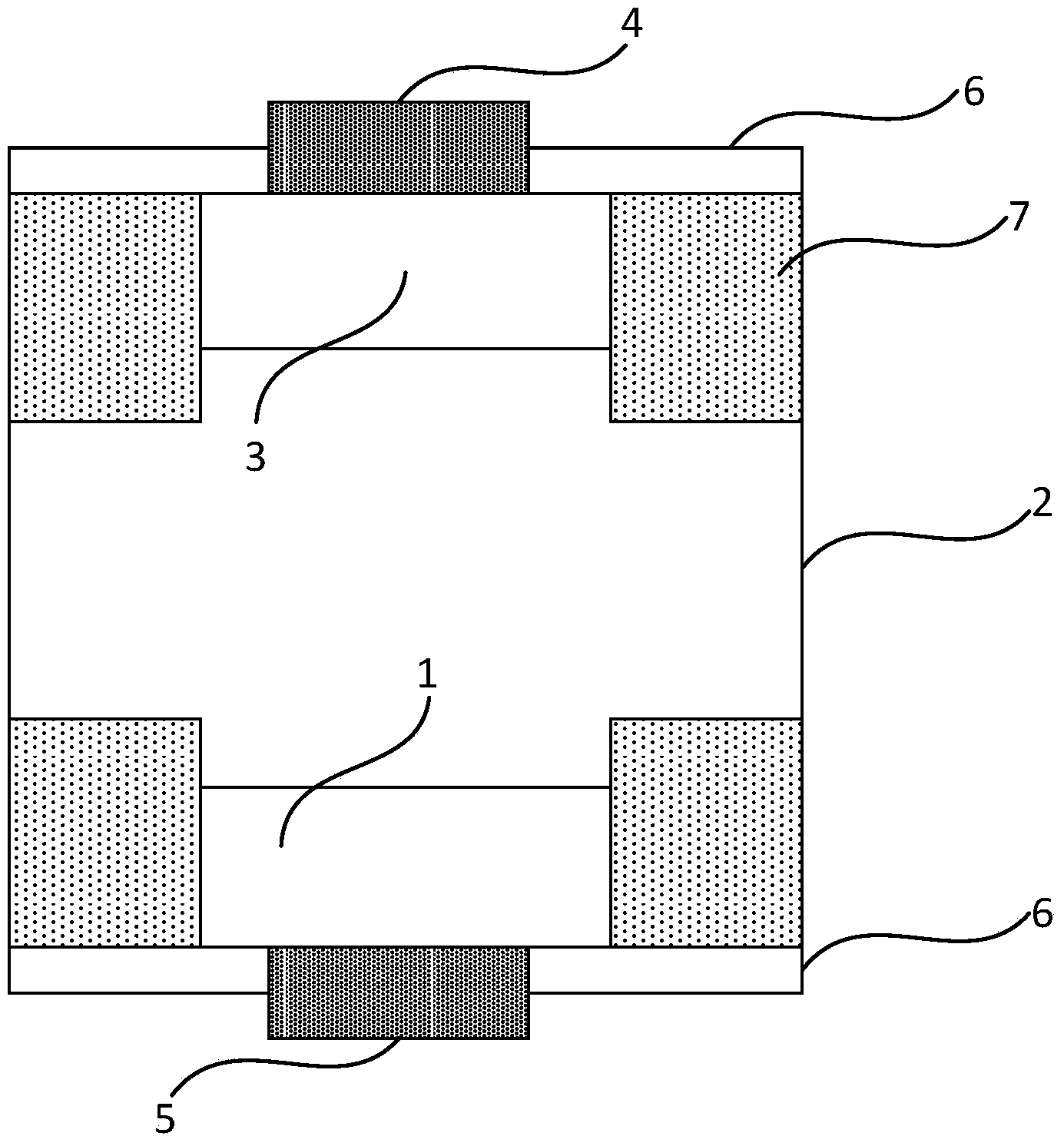
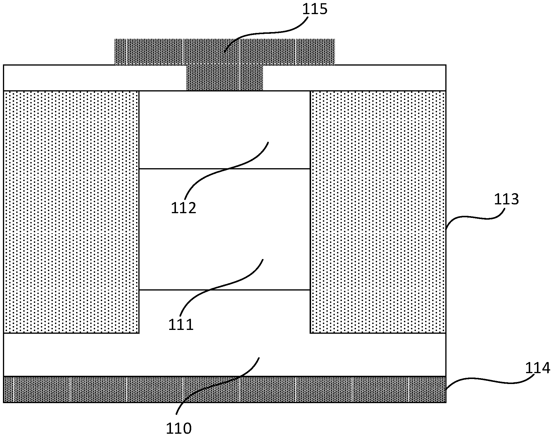
[0057] refer to Figure 3-6 , the manufacture method of bidirectional TVS diode of the present invention, comprises the following steps:

[0058] forming a second conductivity type epitaxial layer 101 on a first conductivity type substrate 100;

[0059] Photolithography and dry etching processes form a plurality of trenches 103 in the second conductivity type epitaxial layer 101, and each trench 103 passes through the second conductivity type epitaxial layer 101 and extends to the first conductivity type substrate middle bottom 100;

[0060] filling each trench 103 with an oxide layer by chemical vapor deposition;

[0061] Doping t...


PUM


Abstract

The invention discloses a bidirectional TVS and a manufacturing method of the bidirectional TVS. The bidirectional TVS comprises a first conduction type substrate, a second conduction type base region, a first conduction type conducting layer, a plurality of grooves, oxide layers, a first electrode and a second electrode, wherein the second conduction type base region is formed on the first conduction type substrate, the first conduction type conducting layer is formed on the second conduction type base region, the grooves all penetrate through the first conduction type conducting layer and the second conduction type base region, extend into the first conduction type substrate, and are filled with the oxide layers, the first electrode is formed on the first conduction type conducting layer, and the second electrode is formed on the back face of the first conduction type substrate. According to the bidirectional TVS and the manufacturing method of the bidirectional TVS, lateral side isolation of a PN junction is achieved through a deep groove structure, the grooves are filled with isolation materials, and electric leakage from the lateral side of the PN junction is reduced; the relevance between the widths of the isolation grooves and the depths of the isolation grooves is greatly reduced, and the size of a chip of the bidirectional TVS is easily reduced.

Description

technical field [0001] The invention relates to a bidirectional TVS diode and a manufacturing method thereof, in particular to a bidirectional TVS diode with a groove and a manufacturing method thereof. Background technique [0002] Bidirectional TVS diodes, that is, bidirectional transient voltage suppression diodes, can be used in various overvoltage protection circuits. Since its structure is designed as a nearly symmetrical NPN three-layer structure, compared with unidirectional protection diodes, bidirectional TVS diodes can conduct in both directions, regardless of the polarity of the voltage applied to both ends, as long as the voltage is greater than Vtrig (reverse trigger voltage ) can be turned on, has a bidirectional overvoltage protection function, has higher flexibility and reliability in use, and can be used as an overvoltage protection device in lithium battery charging, timing, and different circuits. Since its breakdown conduction process presents negative ...

Claims


Application Information

Patent Timeline
Patent Type & Authority Applications(China)
IPC IPC(8): H01L29/861H01L29/06H01L29/10H01L21/329
CPCH01L29/861H01L29/0642H01L29/6609
Inventor 倪凯彬许成宗黄海员顾建平
Owner WILL SEMICON (SHANGHAI) CO LTD
Why Eureka
Try Eureka