Apparatus and method for manufacturing electronic component

A technology for electronic components and manufacturing devices, applied in the direction of electrical components, semiconductor/solid-state device manufacturing, manufacturing tools, etc., can solve the problems of curling, complex cutting knife structure, unsatisfactory blade, etc. Effect

Active Publication Date: 2014-06-11
TOWA
View PDF7 Cites 6 Cited by
  • Summary
  • Abstract
  • Description
  • Claims
  • Application Information

AI Technical Summary

Problems solved by technology

The first problem is that curling (defect) occurs in the slice near the cut surface (for example, refer to paragraph [0090] of Patent Document 3)
The second problem is that "burrs" composed of the substrate (including metal foil such as copper foil provided on the substrate) and the sealing resin are generated on the end surface of the cut chip (hereinafter, the end surface is referred to as the cut surface). (For example, refer to paragraphs [0011] to [0012] of Patent Document 2, and paragraph [0012] of Patent Document 3)
[0014] However, in the first countermeasure, since the two cutting blades are driven, the cutting device becomes complicated and the drive control of the two cutting blades becomes unsatisfactory.
On the other hand, in the second countermeasure, although the cutting knife is maintained as one knife, the structure of one cutting knife (blade) becomes complicated and it is necessary to prepare multiple types corresponding to the combination of a plurality of different materials constituting the resin package. Unsatisfactory problems with blades

Method used


Image

  • Apparatus and method for manufacturing electronic component
  • Apparatus and method for manufacturing electronic component
  • Apparatus and method for manufacturing electronic component

Examples


Embodiment 1

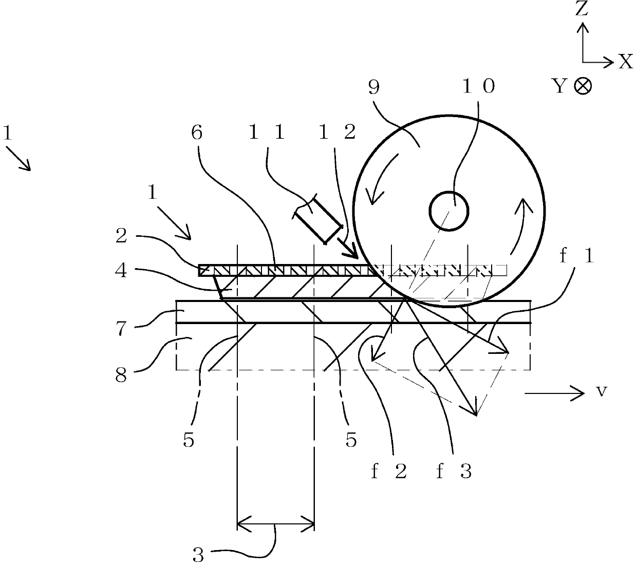
[0072] refer to figure 2 , the method of manufacturing an electronic component according to Embodiment 1 of the present invention, and more specifically, the method of cutting an electronic component will be described. According to the present embodiment, the resin package 1 having a double-layer structure as an object to be cut is cut in two steps. The control part CTL is a control mechanism which controls at least the rotation direction and rotation speed of the rotary knife 9, and the relative movement direction and movement speed of the table 8 and the rotation shaft 10 (spindle). The resin package 1 has: a substrate 2 having a plurality of regions 3; chip-like elements mounted on the plurality of regions 3; The lowermost layer of the resin package 1 is set as the uppermost layer. Furthermore, a rotational axis 10 is provided on the mandrel. The mandrel is omitted from the illustration. In addition, the chip-shaped element is not exposed on the surface of the resin pa...

Embodiment 2

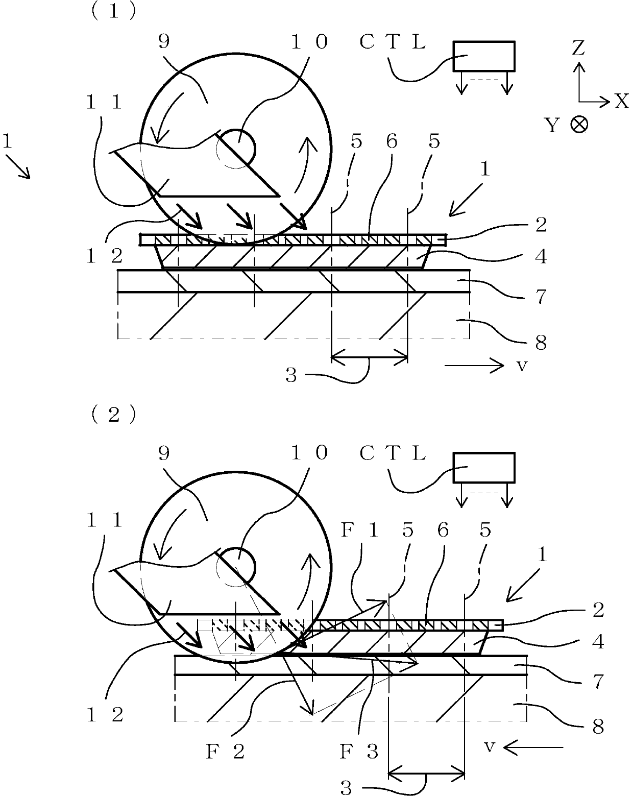
[0087] refer to image 3 , the cutting method for electronic component manufacturing according to Embodiment 2 of the present invention will be described. According to the present embodiment, the resin package 1 having a double-layer structure as an object to be cut is cut in two steps. The difference between the present embodiment and the first embodiment is that the posture in which the resin package 1 is fixed on the upper surface of the table 8 is reversed in the Z direction. In addition, in the present embodiment, the structure of the nozzle 11 and the ejection of the cutting fluid 12 using the nozzle 11 are implemented as in the first embodiment. For this reason, in the following description, the description related to the ejection of the cutting fluid 12 using the nozzle 11 will be omitted.

[0088] Such as image 3 As shown in (1), in this embodiment, the entire thickness of the encapsulating resin 4 (uppermost layer in this embodiment) in the resin package 1 is cut a...

Embodiment 3

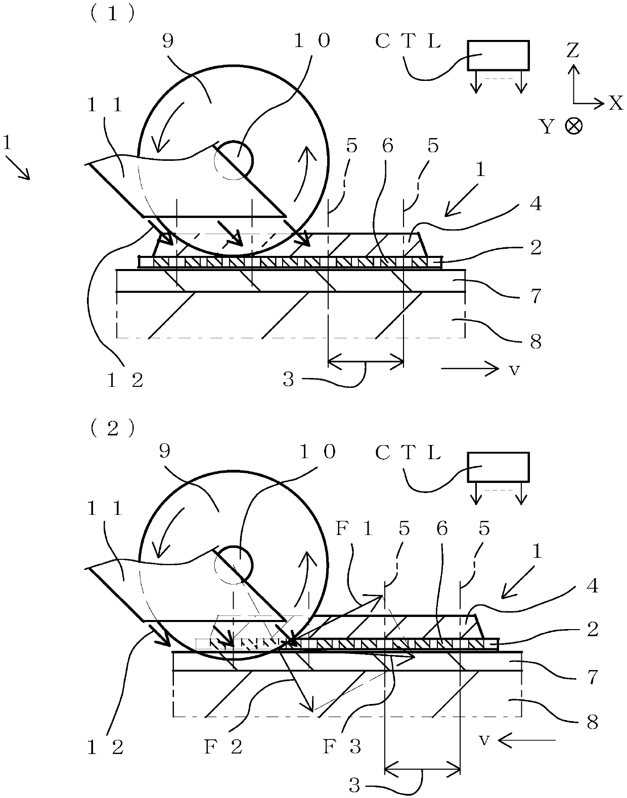
[0103] refer to Figure 4 , the cutting method for electronic component manufacturing according to Embodiment 3 of the present invention will be described. In this embodiment, the resin package 13 which is the object to be cut is cut in three steps. The difference between this embodiment and Embodiment 1 is that the resin package 13 has a three-layer structure. Such as Figure 4 As shown, the resin package 13 has a substrate 2 (the lowermost layer in this embodiment), a reflection member 14 (the middle layer in this embodiment) and encapsulating resin 4 (the uppermost layer in this embodiment) A three-layer structure is formed.

[0104] Such as Figure 4 As shown, a concave portion 15 is formed in the reflection member 14 . The concave portion 15 is provided on each of the plurality of regions 5 provided on the substrate 2 . In each recess 15, the upper surface of the substrate 2 is exposed. Die bonding pads 16 and wire bonding pads 17 are formed on the exposed upper su...


PUM


Abstract

In a state that the periphery of a rotary knife can rotate and cut in a direction being from a surface (upper surface) of a substrate as the top layer to inner side, a workbench moves in a +X direction and the rotary knife cuts the substrate. Secondly, in a state that the periphery of the rotary knife can cut in a direction being from a surface (lower surface) of a packaging resin as a lowest layer to the inner side, the workbench moves in a -X direction and the rotary knife cuts the packaging resin, and therefore a bilayer-structure resin packaged body composed of the substrate and the packaging resin is cut off. Thus, roll rims and 'burrs' which can be generated when the bilayer-structure resin packaged body is cut off once by the rotary knife are prevented.

Description

technical field [0001] The present invention relates to an electronic component manufacturing apparatus and a manufacturing method used when cutting a resin package having a substrate, a plurality of chip-shaped components, and a sealing resin to manufacture a plurality of electronic components. Background technique [0002] When manufacturing electronic components, a technique of cutting a resin package by using a rotary knife (blade) to singulate a plurality of electronic components is widely practiced (for example, refer to Patent Document 1). A resin package as an object to be cut has: a substrate having a plurality of regions; a plurality of chip-like elements mounted in a plurality of regions of the substrate; on the substrate. In this manner, the resin package is a composite material in which a substrate on which a plurality of chip-shaped components is mounted and an encapsulating resin are laminated. [0003] The substrate includes a lead frame made of copper and ...

Claims


Application Information

Patent Timeline
Patent Type & Authority Applications(China)
IPC IPC(8): H01L21/67H01L21/304
CPCH01L2224/45144H01L2224/48091H01L2224/97H01L2924/181H01L2924/00012H01L2924/00014H01L2924/00H01L21/67092B28D5/0058H01L21/78
Inventor 中河原秀司天川刚
Owner TOWA
Why Eureka
Try Eureka