LED packaging method

A technology of LED packaging and packaging methods, which is applied in the direction of electrical components, circuits, semiconductor devices, etc., can solve problems affecting the reliability of LED products, manufacturing cost and price obstacles, and small production capacity of LED products, so as to facilitate large-scale integrated packaging, Reduced packaging cost and low cost effect

Inactive Publication Date: 2014-06-11
SHANGHAI REFOND OPTOELECTRONICS
View PDF6 Cites 4 Cited by
  • Summary
  • Abstract
  • Description
  • Claims
  • Application Information

AI Technical Summary

Problems solved by technology

Due to the different thermal expansion coefficients of brackets, fluorescent glue, and colloids used to bond chips, it is easy to have reliability problems in brackets, fluorescent glue, gold wires, colloids, etc.; and there are many types of LED brackets, bonding wafers and brackets. Most of the materials are PPA, PCT and EMC materials, and their high temperature resistance and air tightness have relatively large defects, which will affect the reliability of LED products.
Although the ceramic bracket has good high temperature

Method used


Image

  • LED packaging method
  • LED packaging method
  • LED packaging method

Examples


Embodiment Construction

[0032] In order to make the object, technical solution and advantages of the present invention clearer, the present invention will be further described in detail below in conjunction with the accompanying drawings and embodiments. It should be understood that the specific embodiments described here are only used to explain the present invention, not to limit the present invention.

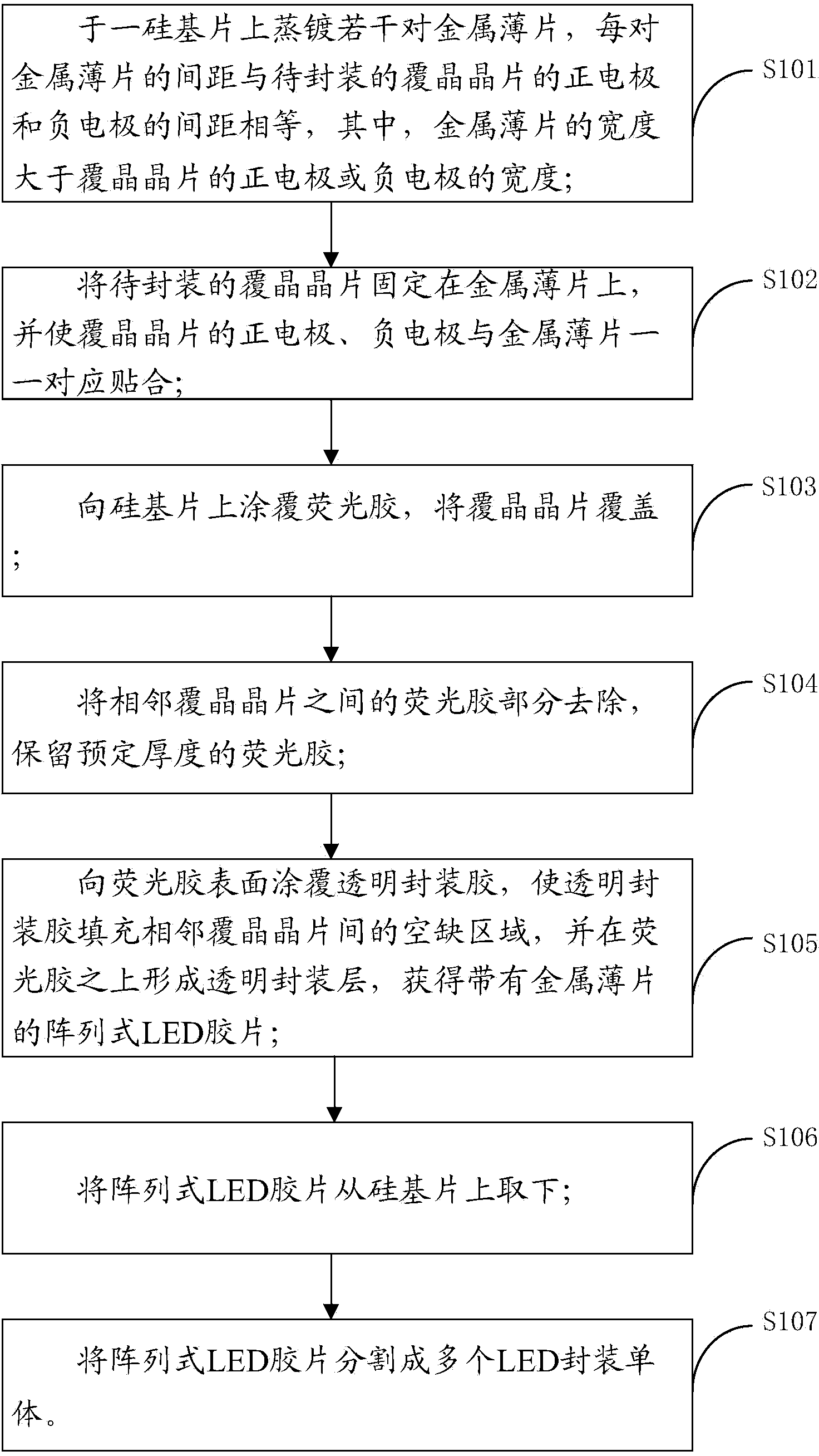
[0033] figure 1 A flow chart of the LED packaging method provided by the embodiment of the present invention is shown, Figure 2b~2h A product package structure diagram corresponding to the method is shown, and for convenience of description, only parts related to this embodiment are shown.

[0034] combine figure 1 , the LED packaging method provided by the embodiment of the present invention includes the following steps:

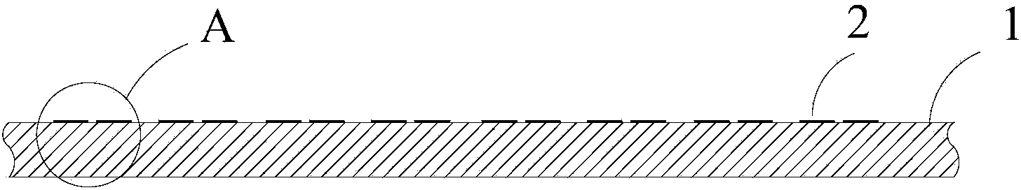
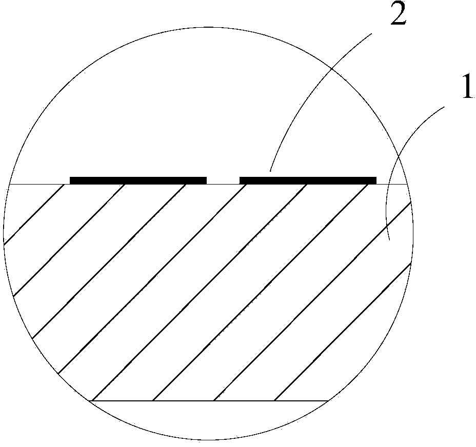
[0035] Step S101, vapor-depositing several pairs of metal sheets 2 on a silicon substrate 1, the distance between each pair of metal sheets 2 is slightly larger than the dis...


PUM

PropertyMeasurementUnit
Thicknessaaaaaaaaaa
Thicknessaaaaaaaaaa
Thicknessaaaaaaaaaa

Abstract

The invention provides an LED packaging method suitable for the LED field. The LED packaging method includes the following steps that a silicon chip is provided with metal sheets in a vapor deposition mode, wherein the distance between each pair of metal sheets equals the distance between the positive electrode of each flip-chip wafer and the negative electrode of the flip-chip wafer, and the width of each metal sheet is larger than that of the positive electrode and that of the negative electrode; the flip-chip wafers are fixed to the metal sheets to make the positive electrodes and the negative electrodes in one-to-one correspondence to the metal sheets; the silicon chip is coated with fluorescent adhesives; the fluorescent adhesives between adjacent flip-chip wafers are removed; transparent packaging adhesives are applied, and an array-type LED film is obtained; the array-type LED film is taken down and cut into a plurality of LED packaging single bodies. According to the LED packaging method, because the flip-chip wafers are packaged on the silicon chip and a packaging body is only composed of the flip-chip wafers, the fluorescent adhesives, the transparent packaging adhesives and the metal sheets, reliability is high, materials are saved, and cost is low. Limitations on shapes of supports do not exist, and therefore large-scale integrated packaging is facilitated; loss caused by scattering-in of photons in fluorescent powder is reduced, and therefore product brightness can be conveniently improved; because it is not needed that the bottoms of the wafers are coated with Au-Sn alloy layers, cost is reduced.

Description

technical field [0001] The invention relates to the technical field of LED product manufacturing, in particular to an LED packaging method. Background technique [0002] The packaging method of traditional white LED products is to fix the LED chip in the cup on the bracket by bonding or eutectic welding, and use gold wires to connect the positive pole of the chip to the positive pole of the bracket, and connect the negative pole of the chip to the On the negative pole of the bracket, fill the bowl with fluorescent glue that matches the target color area. Due to the different thermal expansion coefficients of brackets, fluorescent glue, and colloids used to bond chips, it is easy to have reliability problems in brackets, fluorescent glue, gold wires, colloids, etc.; and there are many types of LED brackets, bonding wafers and brackets. Most of the LED materials are PPA, PCT and EMC materials, and their high temperature resistance and air tightness have relatively large defec...

Claims


Application Information

Patent Timeline
IPC IPC(8): H01L33/48H01L33/50H01L33/54
CPCH01L33/486H01L33/50H01L33/54H01L33/62H01L2933/0033H01L2933/0041H01L2933/005
Inventor 裴小明曹宇星
Owner SHANGHAI REFOND OPTOELECTRONICS
Why Eureka
Try Eureka