

Deep level transient spectroscopy technology based ionizing radiation damage defect detecting method for bipolar devices
A technology of bipolar devices and ionizing radiation, applied in the field of electronics, can solve the problem that the damage defects of bipolar transistors cannot be quantified due to ionizing radiation
- Summary
- Abstract
- Description
- Claims
- Application Information
AI Technical Summary
Problems solved by technology
Method used
Image

Examples
specific Embodiment approach 1
[0036] Specific implementation mode 1: A method for detecting ionizing radiation damage defects of bipolar devices based on deep-level transient spectrum technology described in this implementation mode, the specific process of the method is:
[0037] The first step is to conduct ionizing radiation tests on the bipolar devices, and install the bipolar devices on the low-temperature test bench of the deep-level transient spectrometer to ensure the low-temperature test of the bipolar devices and the deep-level transient spectrometer The platform is tightly connected, and the base and collector of the bipolar device are respectively connected to the high and low test connectors of the deep-level transient spectrometer;
[0038] The second step is to set the test parameters, which include the reverse bias voltage V R , pulse voltage V P , test cycle T W , pulse width T P and temperature sweep range, and guaranteed reverse bias V R -20V to +20V, pulse voltage V P -3V to +3V, t...
specific Embodiment approach 2
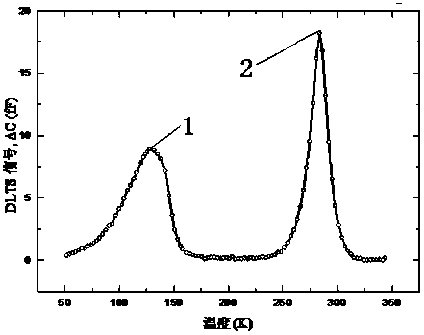
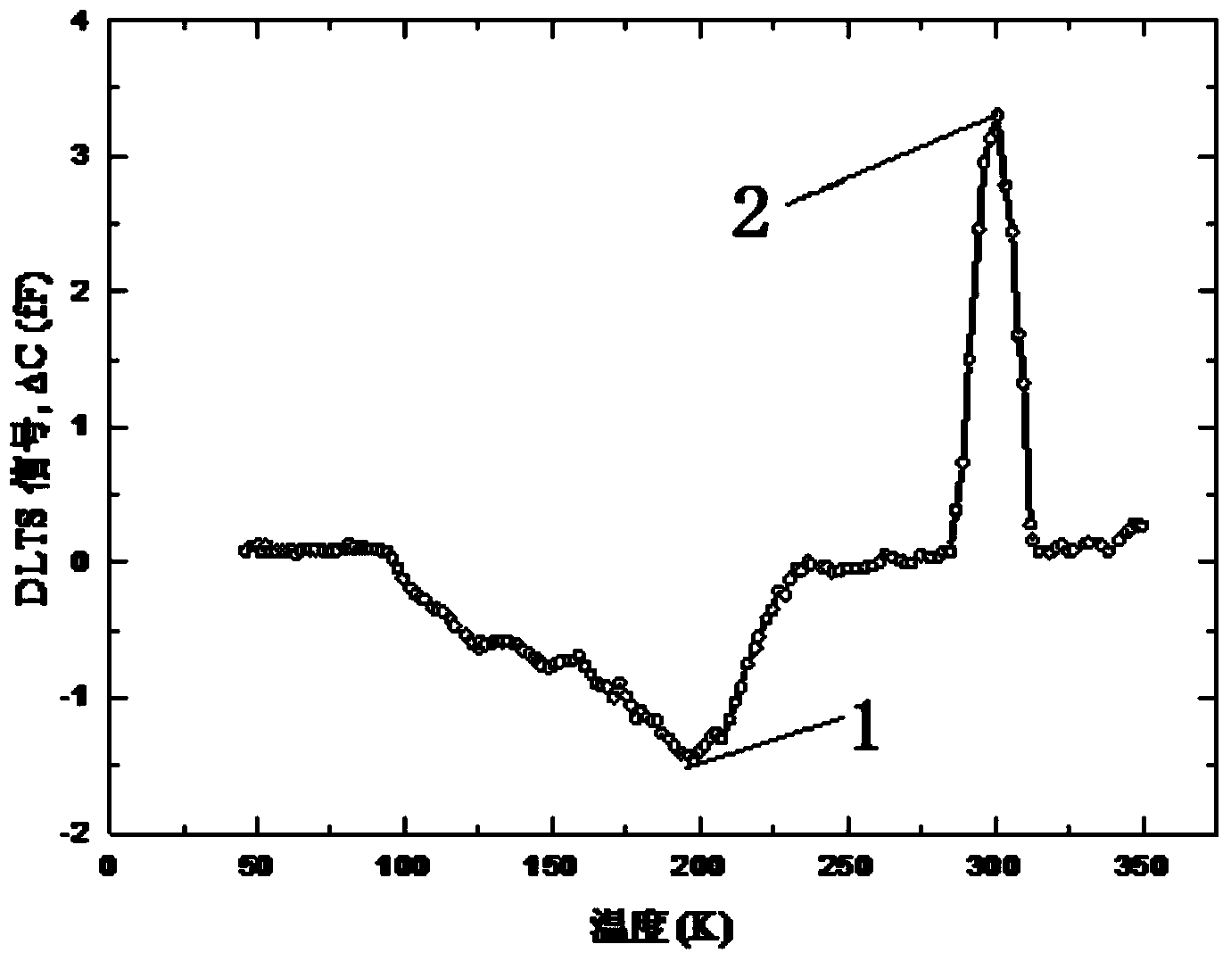
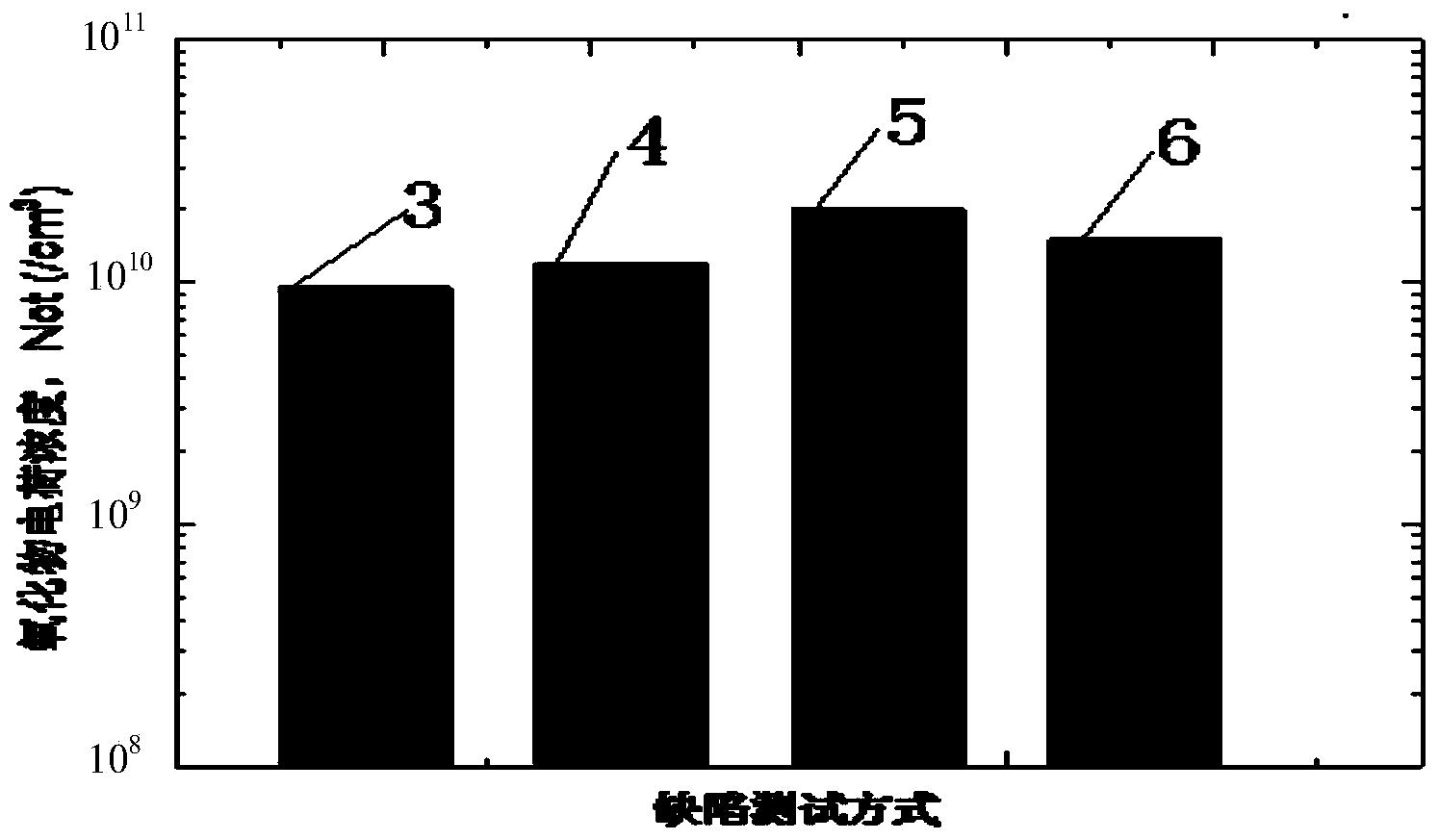
[0041] Embodiment 2: The difference between this embodiment and the method for detecting defects of ionizing radiation damage of bipolar devices based on deep-level transient spectrum technology described in Embodiment 1 is that the ionizing radiation damage of bipolar devices The defect is the defect concentration, and the defect concentration includes the defect concentration of the oxide charge of the bipolar device and the defect concentration of the interface state, wherein: the defect concentration of the oxide charge of the bipolar device is
[0042] N T 1 = 2 N D ΔC 1 C R 1 (formula one),
[0043] Among them, ΔC 1 is the peak height of the DLTS signal peak of the oxide charge, C R1 Indicates the...
specific Embodiment approach 3
[0047] Embodiment 3: The difference between this embodiment and the method for detecting defects of ionizing radiation damage of bipolar devices based on deep-level transient spectrum technology described in Embodiment 1 is that the ionizing radiation damage of bipolar devices The defect is a defect energy level, and the defect energy level includes the defect energy level of the oxide charge of the bipolar device and the defect energy level of the interface state, wherein: the defect energy level of the oxide charge of the bipolar device is
[0048] E. T1 =f(T W ) T 1 (Formula 3),
[0049] Among them, f(T W ) represents the defect energy level factor, T 1 is the temperature corresponding to the DLTS signal peak of the oxide charge,
[0050] The defect energy level of the interface state of the bipolar device is
[0051] E. T2 =f(T W ) T 2 (Formula 4);
[0052] T 2 Indicates the temperature corresponding to the DLTS signal peak of the interface state.
PUM
 Abstract
Description
Claims
Application Information