Photomask and its design method

A design method and technology of photomasks, applied in optomechanical equipment, optics, originals for optomechanical processing, etc., can solve problems such as influence, influence on bonding of solder balls and substrate 1, influence on solder ball filling, etc.

Active Publication Date: 2017-03-29
SEMICON MFG INT (SHANGHAI) CORP
View PDF4 Cites 0 Cited by
  • Summary
  • Abstract
  • Description
  • Claims
  • Application Information

AI Technical Summary

Problems solved by technology

[0006] Because in the subsequent packaging process, solder balls will be filled in the groove 4, the existence of the lift 21 will affect the filling of the solder balls, such as easy to cause voids in the solder balls, affecting the combination of the solder balls and the substrate 1, etc., resulting in Detrimental effects on the subsequent packaging process

Method used


Image

  • Photomask and its design method
  • Photomask and its design method
  • Photomask and its design method

Examples


Embodiment Construction

[0044] In order to make the objectives, technical solutions and advantages of the present invention clearer, the present invention will be described in further detail below with reference to the accompanying drawings and examples.

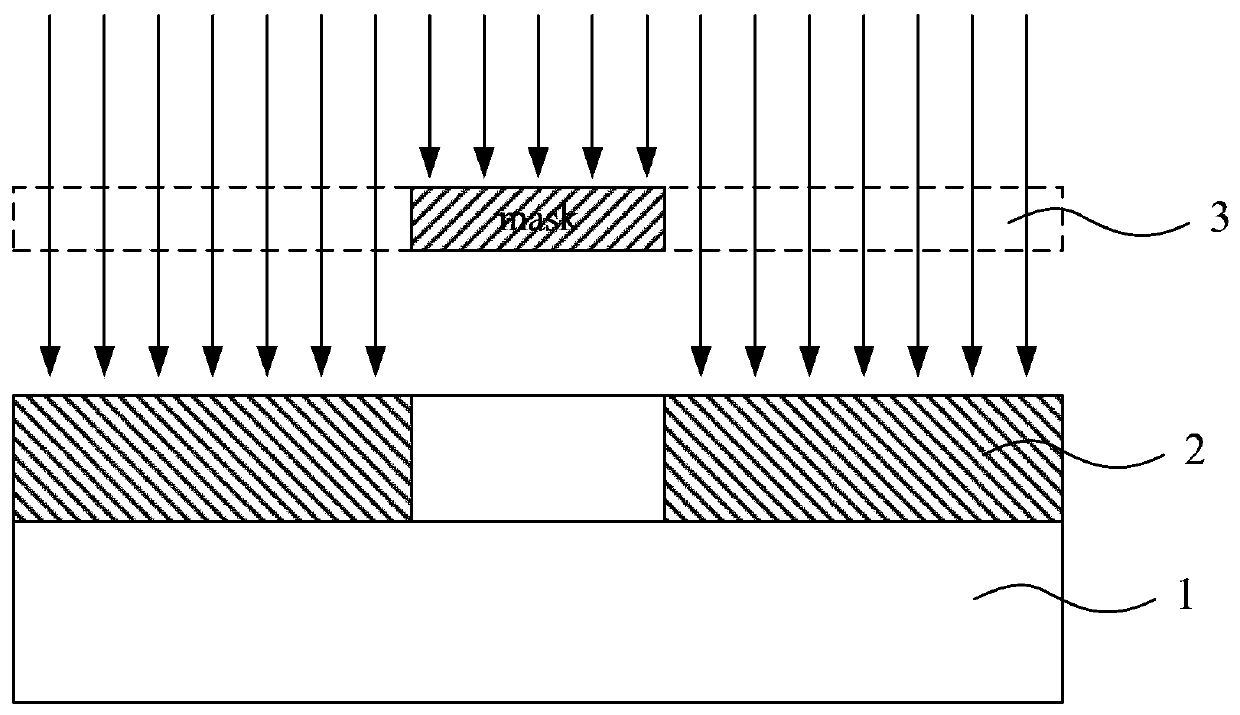
[0045] like Figure 4 As shown, the mask 3 provided by the present invention includes a light-transmitting portion 31 and an opaque portion 32 that form a mask pattern, and the light-transmitting portion 31 is provided with diffraction adjacent to the edge of the opaque portion 32. The grating structure region 33 . like Figure 5 As shown, the grating stripes of the diffraction grating structure region 33 are parallel to the edge of the opaque portion 32 adjacent to the diffraction grating structure region 33 .

[0046] like Image 6 As shown, it is a schematic diagram of exposing the polyimide film 2 by using the photomask 3 of the present invention. Because the diffraction grating structure region 33 exists in the photomask 3 of the present i...


PUM


Abstract

The invention discloses a light shield and its designing method. The light shield comprises a transparent part and a lightproof part forming a light shield pattern, the transparent part is partially provided with a diffraction grating structure area adjacent to the edge of the lightproof part, and the grating strip of the diffraction grating structure area parallels to the edge of the adjacent lightproof part. The diffraction grating structure area adjacent to the edge of the lightproof part is designed in the transparent part of the light shield, so the energy of the area exposed to a polyimide film changes, thereby the morphology of the exposed polyimide film is changed, the polyimide film with no tilting can be obtained after heating curing treatment, and an unfavorable influence of tilting on filing solder balls in the subsequent packaging process of an IC circuit is solved.

Description

technical field [0001] The present invention relates to semiconductor manufacturing technology, in particular to a photomask used in lithography at the packaging stage in an IC manufacturing process and a method for designing the photomask. Background technique [0002] In semiconductor manufacturing technology, in the packaging stage of IC (integrated circuit, integrated circuit), a layer of polyimide (polyimide) film is coated on the surface of the substrate containing the chip to protect the substrate; The polyimide film is exposed, developed and heated and cured by etching means, and finally a groove is formed in the required part of the polyimide film to expose the part of the conductive layer in the substrate that needs to be electrically connected to the outside world; then fill the groove with solder balls for electrical connection with the outside world. After the polyimide film is heated and cured, some undesired changes will occur in its morphology, so the existi...

Claims


Application Information

Patent Timeline
Patent Type & Authority Patents(China)
IPC IPC(8): G03F1/48G03F7/00
Inventor 曹存朋朱晓峥
Owner SEMICON MFG INT (SHANGHAI) CORP
Why Eureka
Try Eureka