Satellite navigation three-dimensional chip and manufacture method thereof

A three-dimensional chip and satellite navigation technology, applied in the field of satellite navigation, can solve the problems of insufficient connection between the radio frequency chip and the core algorithm of the baseband processing chip, restricting the rapid development of the Beidou satellite navigation industry, and high size and power consumption development costs, and achieves a reduction of two Secondary development difficulty, area and volume reduction, and the effect of increasing speed

Inactive Publication Date: 2014-06-18
BEIJING TIANZHONGLEI INTELLIGENT TECH
View PDF0 Cites 1 Cited by
  • Summary
  • Abstract
  • Description
  • Claims
  • Application Information

AI Technical Summary

Problems solved by technology

At present, the terminal application development of domestic Beidou satellite navigation is biased. Some focus on the development of radio frequency chips, and some focus on baseband processing chips. Few can provide independent integrated solutions for radio frequency and baseband processing chips. As a result, the core algorithms of the RF chip and the baseband processing chip are not well connected, and the performance of module development is also greatly reduced.
At the same time, since packaged radio frequency and baseband discrete chips are currently used for secondary development to realize the Beidou satellite navigation function, the size, power consumption, and development cost of the module are very high, which restricts the high-speed development of the Beidou satellite navigation industry to a certain extent. develop

Method used


Image

  • Satellite navigation three-dimensional chip and manufacture method thereof
  • Satellite navigation three-dimensional chip and manufacture method thereof
  • Satellite navigation three-dimensional chip and manufacture method thereof

Examples


no. 1 example 3

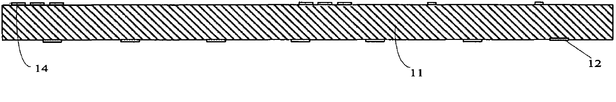
[0040] refer to figure 2 , showing the flow of the three-dimensional chip packaging method according to the first embodiment of the present invention, specifically including:

[0041] Step S101: fixing the first-layer functional chip to a designated position reserved on the substrate;

[0042] In this preferred embodiment, the surface of the first-level chip is pasted on the designated position reserved on the substrate with a placement machine, and then the substrate after the chip is mounted is cured at a high temperature, so that a stable connection is formed between the chip and the substrate;

[0043] Step S102: establishing an electrical connection between the functional chip and the substrate;

[0044] In this preferred embodiment, the pads of the first-level functional chip are led out to the corresponding lead pad positions on the substrate through a wire bonding machine, so as to realize the electrical connection between the first-level functional chip and the subs...


PUM


Abstract

The invention discloses a satellite navigation three-dimensional chip and a manufacture method thereof. The three-dimensional chip comprises one or multiple substrates, bare chips, polymer or support plates, bonding wires or micro salient points, and a BGA solder ball array, wherein the substrates are used for supporting functional chips to realize electrical connection between the functional chips, the bare chips of the radiofrequency, baseband, storage microprocessor and other functional chips are laid on the substrates in a stacked or planar manner, the polymer or carrier plates are positioned between the vertically adjacent functional chips and used for fixing and isolating the functional chips, the bonding wires or micro salient points are used for realizing electrical connection among the functional chips as well as between the functional chips and the substrates, the micro salient points are formed in a flat chip bonding manner, and the BGA solder ball array is arranged the lower surface of the base layer. The multiple functional chips for realizing Beidou&GPS dual-mode satellite navigation are integrated in a packaging body via a series of substrate and micro-assembly technologies to form a small electronic product with high performance, high density and low loss, and the problems that a present satellite navigation product module is large in size, high in development difficulty, high in power consumption cost and the like are solved.

Description

technical field [0001] The invention relates to the technical field of satellite navigation, in particular to a Beidou&GPS dual-mode satellite navigation three-dimensional receiving chip realized by using three-dimensional multi-chip component technology (3D-MCM) and a manufacturing method thereof. Background technique [0002] The Beidou satellite navigation system is a global satellite navigation system with my country's independent intellectual property rights. With the gradual construction and improvement of the Beidou satellite navigation system, the satellite navigation, precise timing and location service industries with Beidou as the core are playing an increasingly important role in the national economic life, becoming a crucial emerging industry, and the development prospects are very broad . [0003] High-performance satellite navigation terminals and chips are the core of satellite navigation systems and the foundation of the entire navigation service industry c...

Claims


Application Information

Patent Timeline
Patent Type & Authority Applications(China)
IPC IPC(8): H01L25/16H01L23/488G01S19/37H01L21/98H01L21/60
CPCH01L2224/48091H01L2224/73265
Inventor 谢伟东潘小山
Owner BEIJING TIANZHONGLEI INTELLIGENT TECH
Why Eureka
Try Eureka