Electrostatic discharge protection circuit and manufacturing method thereof

An electrostatic discharge protection and circuit technology, applied in circuits, electrical components, electrical solid devices, etc., can solve problems such as inability to open conductive channels

Active Publication Date: 2014-06-18
SEMICON MFG INT (SHANGHAI) CORP
View PDF7 Cites 3 Cited by
  • Summary
  • Abstract
  • Description
  • Claims
  • Application Information

AI Technical Summary

Problems solved by technology

Since the gate 101 and the P-type substrate 100 are grounded, the GGNMOS device can never be turned on to form a conductive channel

Method used


Image

  • Electrostatic discharge protection circuit and manufacturing method thereof
  • Electrostatic discharge protection circuit and manufacturing method thereof
  • Electrostatic discharge protection circuit and manufacturing method thereof

Examples


Embodiment Construction

[0031] In order to make the object, technical solution and advantages of the present invention clearer, the present invention will be further described in detail below with reference to the accompanying drawings and examples.
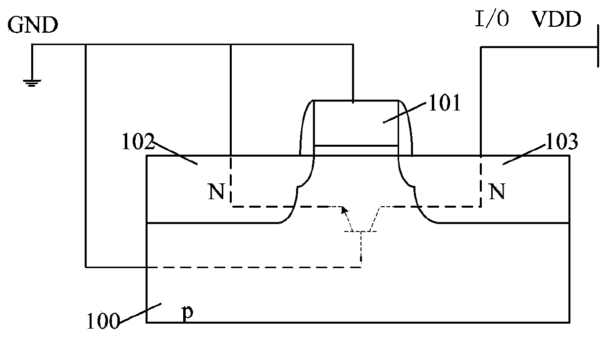
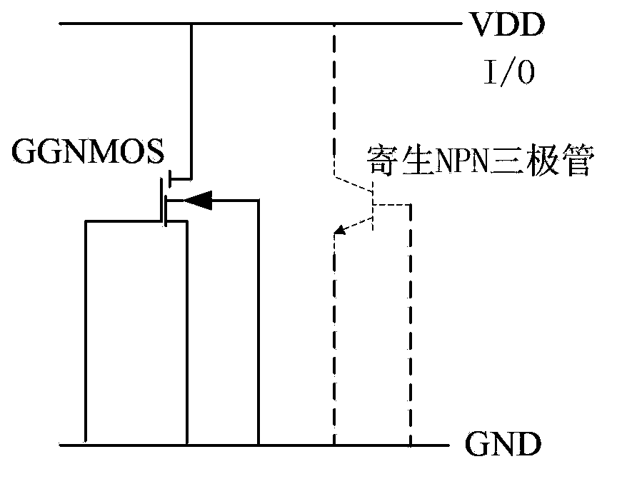
[0032] The core idea of ​​the present invention is to add a Peltier cooling element in the ESD protection circuit with a GGNMOS transistor, the Peltier cooling element is located near the GGNMOS transistor, and the Peltier cooling element can cool the GGNMOS transistor after the current is applied. Effect. The following briefly introduces the application background of Peltier cooling elements.

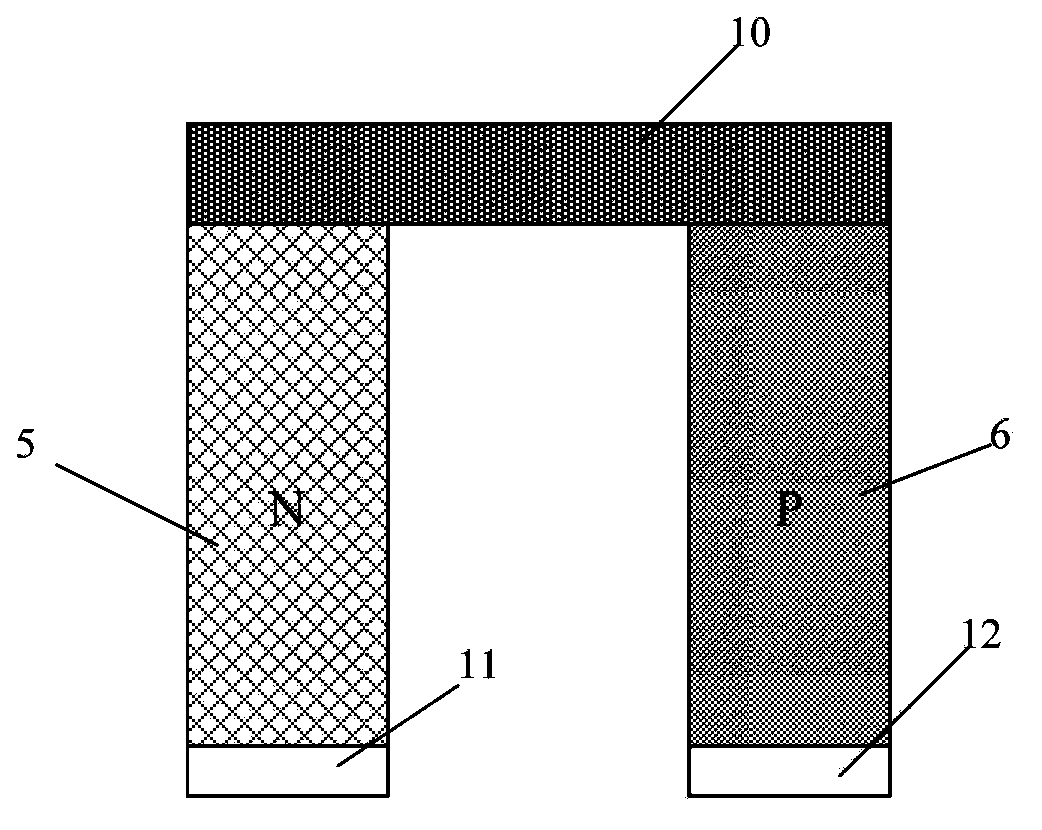
[0033] When an electric current flows through two different conductors that are connected and kept at a uniform temperature, radiated or absorbed heat is generated in addition to Joule heat. This effect was first discovered by J.C.A.Peltier in 1834, and is called the Peltier effect. The schematic diagram of the Peltier cooling element formed according to the P...


PUM


Abstract

The invention discloses an electrostatic discharge protection circuit. The electrostatic discharge protection circuit comprises a gate-grounded N type metal oxide semiconductor (GGNMOS) transistor located on a semiconductor substrate, a drain electrode of the GGNMOS transistor is connected an input/output end of a chip circuit, a source electrode and a gate electrode and the semiconductor substrate are all connected to the ground; and the circuit also comprises a Peltier cooling element that is located near the GGNMOS transsitor and used for absorbing heat generated by the GGNMOS transistor. The invention also discloses a manufacturing method of the electrostatic discharge protection circuit. By adoption of the electrostatic discharge protection circuit, the working life of an ESD protection device can be prolonged.

Description

technical field [0001] The invention relates to the field of integrated circuit manufacturing, in particular to an electrostatic discharge protection circuit and a manufacturing method thereof. Background technique [0002] In integrated circuit (IC) chip manufacturing and final application systems, with the continuous improvement of VLSI process technology, the current complementary metal oxide semiconductor (CMOS) integrated circuit has entered the ultra-deep sub-micron stage, MOS devices The size of ICs continues to shrink, and the harm of Electrostatic Discharge (ESD) to integrated circuits has become more and more significant. According to statistics, 35% of products with integrated circuit failures are caused by ESD problems. Therefore, it is particularly important to design ESD protection for integrated circuits. [0003] When devices are used to protect integrated circuits from ESD, commonly used devices are grounded gate NMOS transistors (GGNMOS), silicon controll...

Claims


Application Information

Patent Timeline
Patent Type & Authority Applications(China)
IPC IPC(8): H01L27/02H01L23/38H01L21/82
CPCH01L2924/0002H01L2924/00
Inventor 甘正浩冯军宏
Owner SEMICON MFG INT (SHANGHAI) CORP
Why Eureka
Try Eureka