Molybdenum film containing sodium and preparation method and application thereof
A molybdenum layer and content technology, applied in the field of sodium-containing molybdenum film and its preparation, can solve problems such as dependence, and achieve a wide range of applications
- Summary
- Abstract
- Description
- Claims
- Application Information
AI Technical Summary
Problems solved by technology
Method used
Image
Examples
Embodiment 1
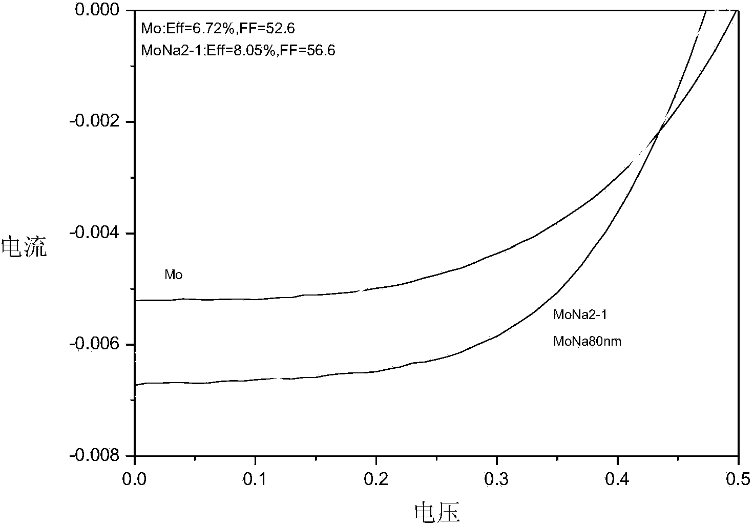
[0026] A layer of pure molybdenum film with a thickness of 800nm is sputtered on the glass substrate by DC magnetron sputtering method. The film adopts a laminated structure, the sputtering power is 180W, the sputtering pressure is 8mTorr for 4min, and the sputtering pressure is 5mTorr for 36min; then DC magnetron sputtering is used to deposit a layer of sodium-molybdenum film with a thickness of 80nm. The sodium-molybdenum target has a Na content of 10%[at], a Mo content of 90%[at], a target diameter of 50.8mm, and a thickness of 6.35mm. The sputtering power used is 100W, the sputtering pressure is 100W, and the sputtering time is 10min; Then sputter a layer of pure molybdenum film with a thickness of 100nm. The Mo content of the molybdenum target used for sputtering is 99.95%[at], the target diameter is 50.8mm, and the thickness is 3.175mm. The molybdenum film adopts a laminated structure, and the sputtering power used 180W, sputtering gas pressure 5mTorr deposition 5min. ...
Embodiment 2
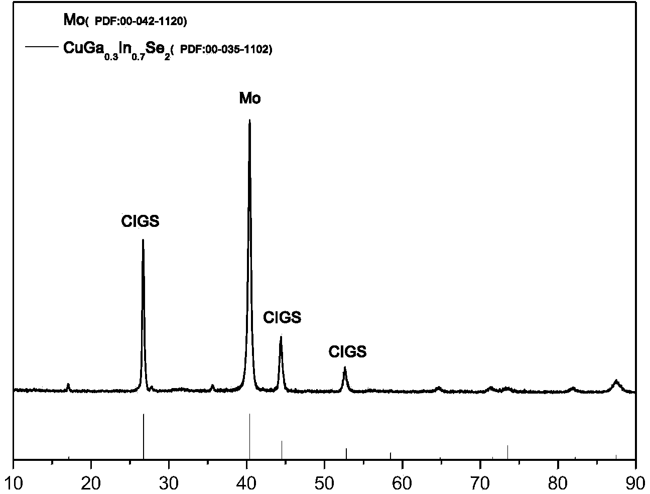
[0029] A layer of pure molybdenum film with a thickness of 800nm is sputtered on the glass substrate by DC magnetron sputtering method. The molybdenum film adopts a stacked structure, the sputtering power is 180W, and the sputtering pressure is 8mTorr for 4min and 5mTorr. Deposit for 36 minutes; then use DC magnetron sputtering to deposit a layer of 80nm thick sodium-containing molybdenum film. The power is 100W, the sputtering pressure is 100W, and the sputtering time is 10min; then a layer of pure molybdenum film with a thickness of 100nm is sputtered. After 5 minutes, a sodium-molybdenum film was obtained. Then, a CuGa / In prefabricated layer structure is prepared by magnetron sputtering on the sodium-containing molybdenum film, and selenized in an annealing furnace to obtain a copper indium gallium selenide thin film.
[0030] By using X-ray diffraction (XRD) to analyze its crystal structure, such as crystal form, crystal orientation, crystal grain stress and other cryst...
PUM
| Property | Measurement | Unit |
|---|---|---|
| Diameter | aaaaa | aaaaa |
| Thickness | aaaaa | aaaaa |
| Thickness | aaaaa | aaaaa |
Abstract
Description
Claims
Application Information


