
High-brightness LED with surface microstructure and manufacturing and screening method thereof

A technology of light-emitting diodes and light-emitting diodes, which is applied to electrical components, circuits, semiconductor devices, etc., can solve problems such as the inability to define the quality of surface microstructures, and achieve the effects of weakening light extraction efficiency, high efficiency, and high accuracy

Inactive Publication Date: 2014-06-18
TIANJIN SANAN OPTOELECTRONICS
View PDF2 Cites 2 Cited by
  • Summary
  • Abstract
  • Description
  • Claims
  • Application Information

AI Technical Summary

Problems solved by technology

[0005] The purpose of the present invention is to provide a high-brightness light-emitting diode with surface microstructure and its preparation and screening method, which is used to improve the yield of high-brightness light-emitting diodes, and at the same time solve the problem that the surface microstructure cannot be defined in the prior art. Bad question

Method used


Image

  • High-brightness LED with surface microstructure and manufacturing and screening method thereof
  • High-brightness LED with surface microstructure and manufacturing and screening method thereof
  • High-brightness LED with surface microstructure and manufacturing and screening method thereof

Examples


Embodiment 1

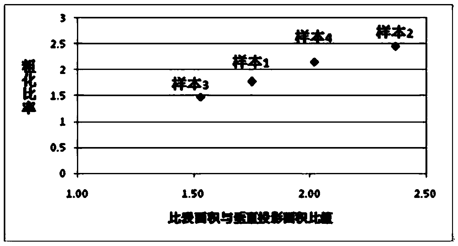
[0054] There are four samples in Example 1. Samples 1-4 are all LEDs with an N-type contact layer on the surface microstructure. The structures are basically the same. The epitaxial wafers are grown by depositing a buffer layer on the epitaxial substrate. (buffer layer) and N-type electrical contact layer, and then deposit an N-type contact layer (n-cladding), deposit a multi-layer quantum well (MQW) structure on the n-cladding, and then deposit a P-type contact layer on the MQW structure ( p-cladding), and finally the electrical contact layer to complete the growth of the epitaxial layer structure; the difference between samples 1-4 is that the materials of each corresponding functional layer are different, so that the wavelengths of light emitted by samples 1-4 are different , the specific functional layer components of samples 1-4 are detailed in Table 1 below:

[0055] Table 1 The composition of each functional layer of sample 1-4

[0056]

[0057] After the epitaxial ...

Embodiment 2

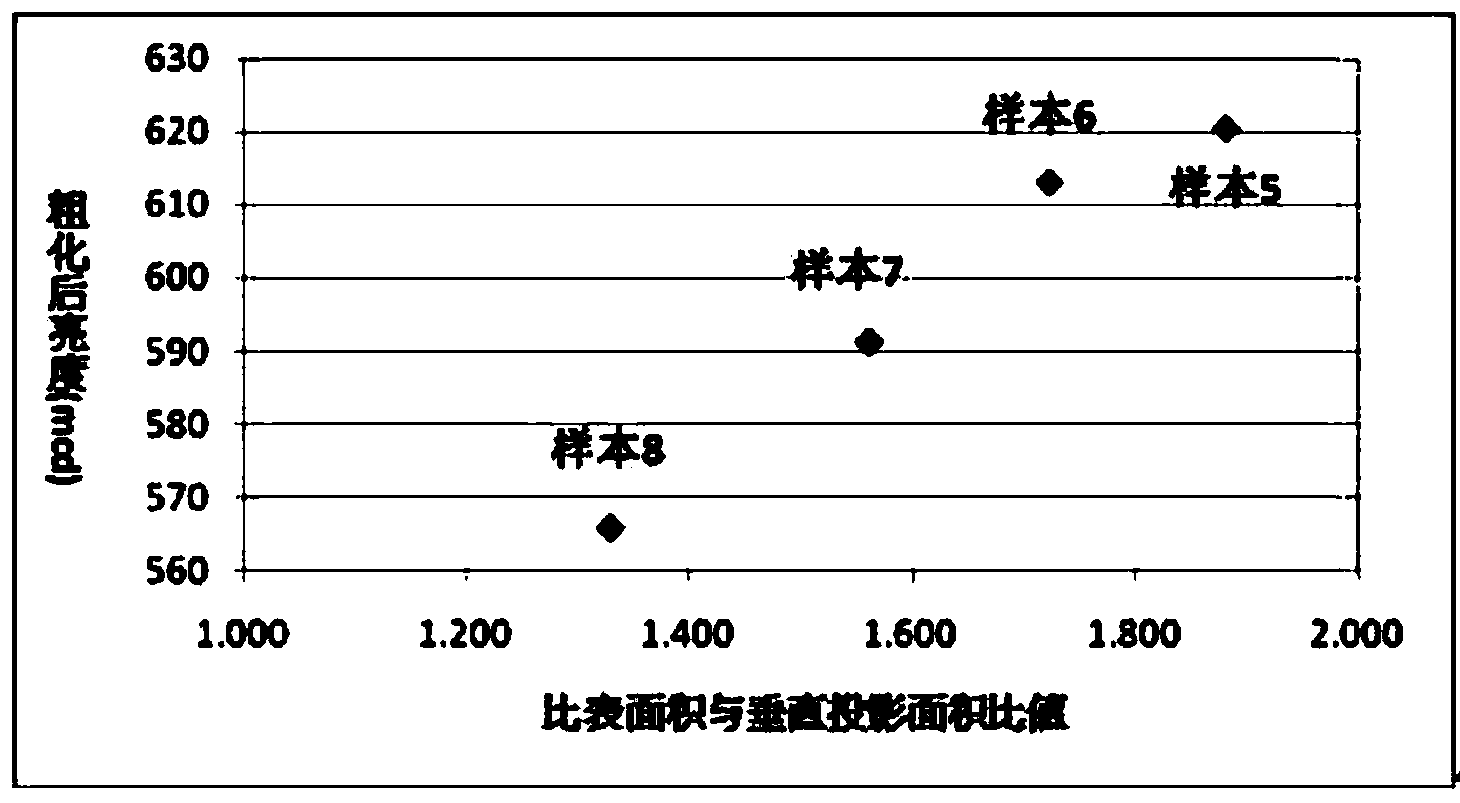
[0069] There are four samples in Example 2, and the preparation method of samples 5-8 is the same, specifically depositing a buffer layer (GaAs) and an electrical contact layer on the epitaxial substrate, and then depositing n-cladding (n-GaAs). MQW (InGaP / AlGaInP) structure is deposited on top of the n-cladding, p-cladding (p-GaP) is deposited on the MQW structure, and finally an electrical contact layer is deposited to complete the growth of the epitaxial layer structure; epitaxial wafers of samples 5-8 After the growth is completed, a wafer that can be roughened is prepared, and then the surface of the wafer is roughened to form samples 5-8 with surface microstructures.

[0070] The surface roughening treatment methods of samples 5-8 are basically the same, including the following steps:

[0071] (1) Expose the light-emitting surfaces that need to be roughened on samples 5-8, and protect the light-emitting surfaces that do not need to be roughened with photoresist or metal;...

Embodiment 3

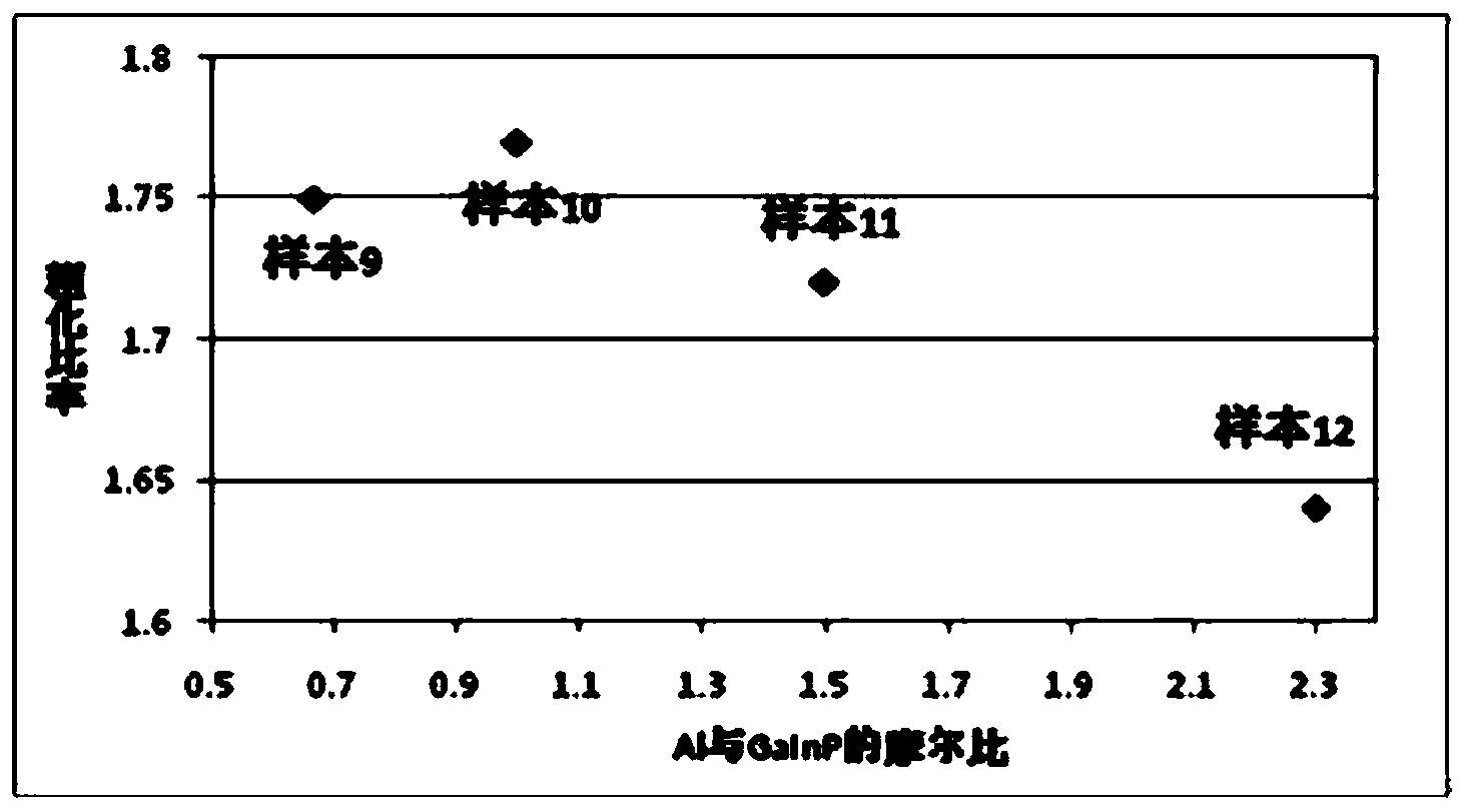
[0080] In Example 3, four samples are included. Samples 9-12 are all epitaxial wafers with a vertical structure, and the preparation method is the same. The specific preparation method is to deposit a buffer layer (GaAs) and an electrical contact layer on the epitaxial substrate, and then Deposit n-cladding (Al X (GaInP) X ), deposit an MQW (InGaP / AlGaInP) structure above the n-cladding, deposit p-cladding (p-GaP) on the MQW structure, and finally an electrical contact layer to complete the growth of the epitaxial layer structure; sample 9- After the epitaxial wafer of 12 is grown, it is prepared into a wafer that can be roughened, and then the surface of the wafer is roughened to form samples 9-12 with a surface microstructure.

[0081] The steps of the coarsening processing method for samples 9-12 are basically the same, including the following steps:

[0082] (1) The light-emitting surfaces that need to be roughened on samples 9-12 are exposed respectively, and the light-...


PUM

PropertyMeasurementUnit
Light intensityaaaaaaaaaa

Abstract

The invention provides a high-brightness LED with a surface microstructure and a manufacturing and screening method of the high-brightness LED. The surface microstructure is characterized in that the ratio of the roughened total surface area of a light emitting surface of the LED to the vertical projection area of the light emitting surface of the LED is larger than 1.5, and the peak density on the light emitting surface is larger than or equal to 0.3 / micron<2>. The larger the ratio of the roughened total surface area of an epitaxial wafer to the vertical projection area of the epitaxial wafer is, the more conveniently the light taking-out efficiency of the epitaxial wafer can be improved; the more the number of peaks with the height larger than a critical height in the unit area is, the more conveniently the light taking-out efficiency of the epitaxial wafer can be improved, and the light taking-out efficiency of the epitaxial wafer is greatly improved.

Description

technical field [0001] The invention belongs to the technical field of semiconductor optoelectronics, and in particular relates to a high-brightness light-emitting diode with a surface microstructure and a preparation and screening method thereof. Background technique [0002] LED is a semiconductor PN junction diode. When a forward voltage is applied to both ends of the PN junction, the carriers are excited from a low-energy state to a high-energy state and return to a low-energy state in an unstable state. According to energy conservation Theorem, excess energy is released in the form of photons. The external quantum efficiency of the LED is the key to improving the luminous efficiency of the LED, and the external quantum efficiency of the LED depends on the internal quantum efficiency of the epitaxial material and the light extraction efficiency of the epitaxial wafer. At present, people are precisely controlling the epitaxial growth, doping concentration and reducing dis...

Claims


Application Information

Patent Timeline
IPC IPC(8): H01L33/22H01L33/00
CPCH01L33/305H01L22/12H01L33/0062H01L33/06H01L33/22H01L33/405H01L2933/0016H01L33/30
Inventor 吴超瑜蔡坤煌卢怡安吴俊毅陶青山王笃祥
Owner TIANJIN SANAN OPTOELECTRONICS
Learn More