
Mems device vacuum packaging structure

A vacuum packaging and device technology, applied in microstructure technology, electric solid device, semiconductor device, etc., can solve the problems of reduced mechanical strength of vacuum packaging of devices, reduced electrical isolation effect of devices, and poor density of through-silicon vias, etc. High density, low contact resistance, good long-term stability

Active Publication Date: 2016-01-20
QST CORP
View PDF9 Cites 0 Cited by
  • Summary
  • Abstract
  • Description
  • Claims
  • Application Information

AI Technical Summary

Problems solved by technology

[0006] In view of the above-mentioned shortcomings of the prior art, the purpose of the present invention is to provide a MEMS device vacuum packaging structure, which is used to solve the problem of device reliability caused by the difference in thermal expansion coefficient between the metal filler formed in the through-silicon via and silicon in the prior art. Reduced performance, poor densification of through-silicon vias used for electrical isolation, reduced electrical isolation of devices, reduced mechanical strength of device vacuum packaging, and low device packaging density

Method used


Image

  • Mems device vacuum packaging structure
  • Mems device vacuum packaging structure
  • Mems device vacuum packaging structure

Examples


Embodiment 1

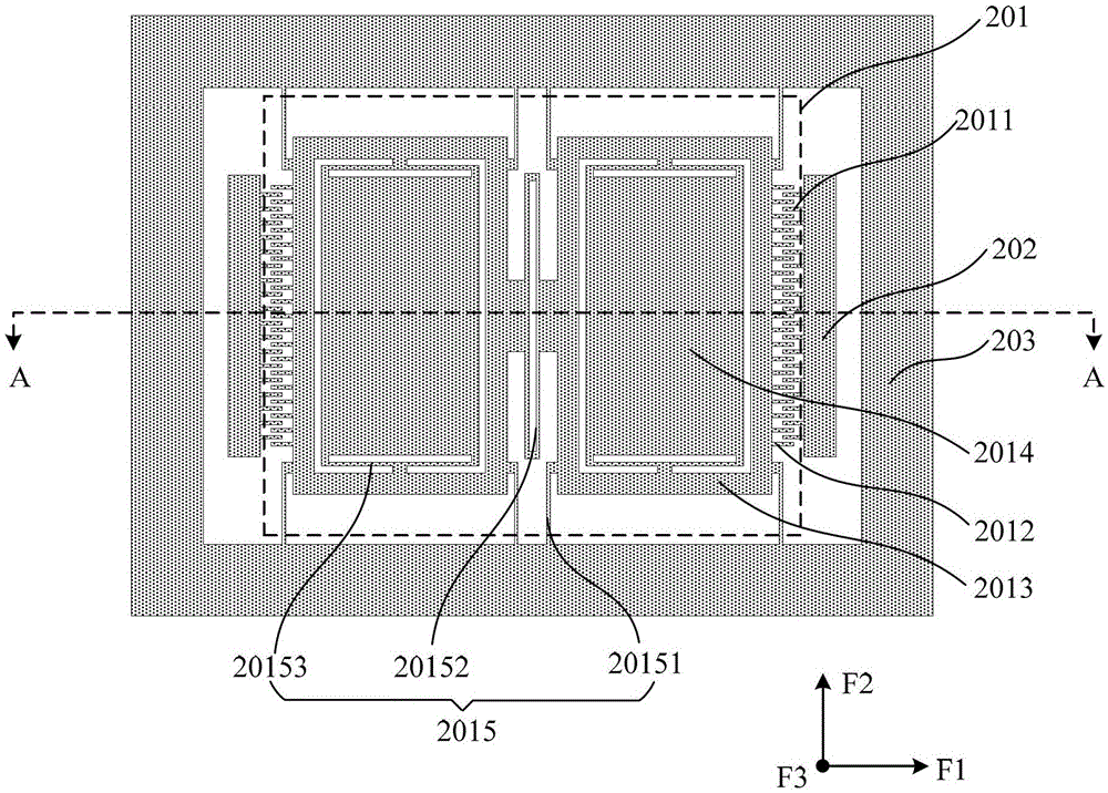
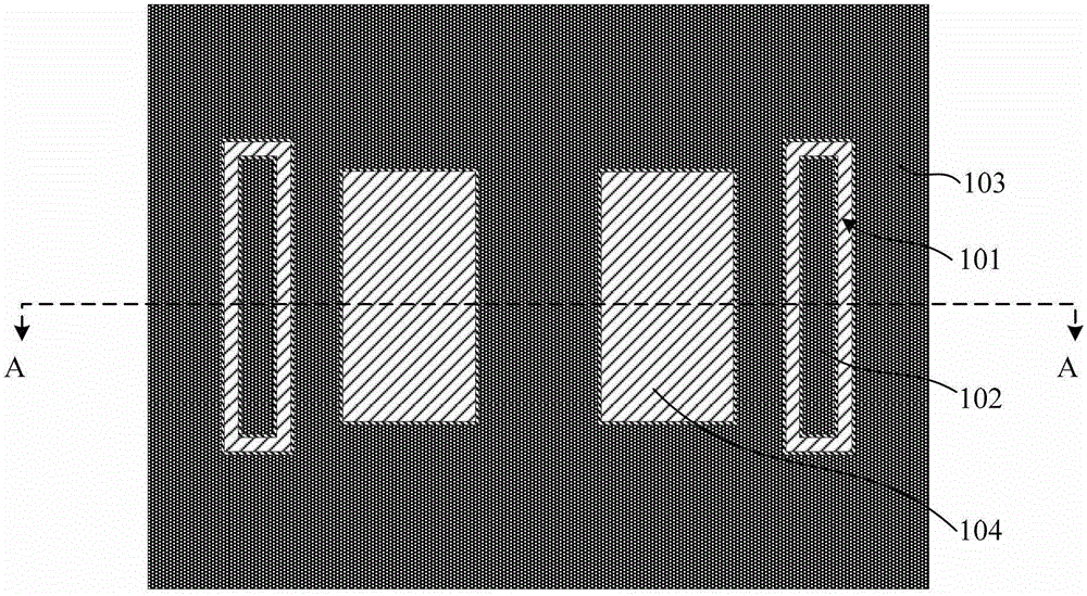
[0076] Such as Figure 1 to Figure 5 As shown, the present invention provides a MEMS device vacuum packaging structure, which at least includes: a substrate 1 , a structural layer 2 , and a cover plate 3 . Wherein, the substrate 1 includes at least an annular isolation structure 101, a first electrode 102, and a frame support structure 103; the structural layer 2 includes at least a frame 203, an electrode connection assembly, and a first region 201 for manufacturing the MEMS device; The cover plate 3 at least includes a first groove 301 . Specifically, in the first embodiment, a micro angular velocity sensor is used as the MEMS device of the structural layer 2 for specific description.

[0077] The structural layer 2 is located on the substrate 1, and at least includes a frame 203 bonded to the inner side of the edge of the substrate 1, an electrode connection assembly of the MEMS device bonded to the first electrode 102, and used to make the The first region 201 of the MEM...

Embodiment 2

[0098] The technical solution of the second embodiment is basically the same as that of the first embodiment, except that the internal structure of the substrate is different. In this second embodiment, only the relevant differences are described, and the same parts as those of the first embodiment are not repeated. A repeat.

[0099] Such as figure 2 , Figure 4 to Figure 7 As shown, the present invention provides a MEMS device vacuum packaging structure, which at least includes: a substrate 1 , a structural layer 2 , and a cover plate 3 . Wherein, the substrate 1 includes at least an annular isolation structure 101, a first electrode 102, and a frame support structure 103; the structural layer 2 includes at least a frame 203, an electrode connection assembly, and a first region 201 for manufacturing the MEMS device; The cover plate 3 at least includes a first groove 301 . Specifically, in the second embodiment, a micro angular velocity sensor is used as the MEMS device o...


PUM


Abstract

The invention provides a vacuum encapsulating structure for an MEMS (Micro Electro Mechanical System) device. The vacuum encapsulating structure at least comprises a substrate, a structural layer and a cover plate. Through holes filled with an epitaxial material and an insulating layer are formed in the substrate, electrical isolation is realized through the insulating material on the side wall of the through hole (annular isolating structure), and the through holes are filled with silicon materials growing in an epitaxial manner, thereby increasing the filler compactness, enhancing the reliability of the vacuum encapsulating structure, and solving the problem of reduction of the reliability due to the difference between the thermal expansion coefficients of a metal filler and silicon. By adopting an all-silicon structure, the vacuum encapsulating structure has the advantages of no outgasing, high long-term stability and high reliability. When an assembly needing a corresponding electrode exists in the MEMS device, a through hole vertically corresponding to the assembly is formed, an epitaxial material in the through hole is taken as a filling electrode, and the filling electrode is an electrode vertically corresponding to the encapsulated MEMS device, thereby increasing the encapsulating density and reducing the encapsulating area of the MEMS device.

Description

technical field [0001] The invention belongs to the field of micro-electro-mechanical systems, and relates to a vacuum packaging structure of MEMS devices. Background technique [0002] Accelerometers and angular velocity meters produced by microelectronic machining technology have been widely used in the fields of car navigation and consumer electronics. These sensors have the advantages of low cost, mass production, and good stability. However, when the mechanical structure reaches the micron level, the air damping effect becomes a key factor affecting the performance of the device. Vacuum packaging can greatly reduce the air damping effect and significantly improve the quality factor of the device. [0003] StevenS.Nasiri and AnthonyFrancisFlannery, JR. proposed a CMOS silicon chip and MEMS silicon chip bonding and packaging structure using through-silicon vias (Method off abrication of Al / Gebonding in wafer packaging enviroment and a product produced therefrom, US2008 / ...

Claims


Application Information

Patent Timeline
Patent Type & Authority Patents(China)
IPC IPC(8): B81B7/00B81C1/00
Inventor 焦继伟王敏昌颜培力秦嵩
Owner QST CORP
Learn More