an image sensor

An image sensor and optical sensor technology, applied in the field of image sensors, can solve the problems of increasing imaging signal residue, slow readout speed of photoelectric signal, and affecting dark current performance, etc., so as to reduce imaging signal residue, difficulty and risk small effect

Active Publication Date: 2017-04-12
SHANGHAI TIANMA MICRO ELECTRONICS CO LTD
View PDF7 Cites 0 Cited by
  • Summary
  • Abstract
  • Description
  • Claims
  • Application Information

AI Technical Summary

Problems solved by technology

[0005] (1) The photoelectric efficiency of the image sensor is mainly determined by the thickness of the p-type silicon layer of the PIN junction diode. Adjusting the photoelectric efficiency can only adjust the thickness of this layer, but adjusting the thickness of the p-type silicon layer will affect the etching process of the PIN junction diode , affecting other properties such as dark current;
[0006] (2) If multiple image sensor products are mixed on the same substrate, the photoelectric conversion efficiency of each image sensor produced is the same, and it is impossible to flexibly adjust the photoelectric conversion efficiency of each image sensor according to different product requirements;
[0007] (3) Due to the high resistivity of P-doped amorphous silicon, the photoelectric signal in the peripheral area of ​​the PIN junction diode is read out very slowly, which increases the residual imaging signal

Method used


Image

  • an image sensor
  • an image sensor
  • an image sensor

Examples


Embodiment Construction

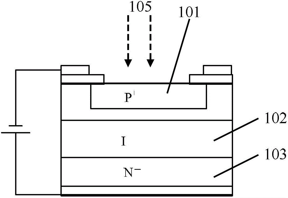
[0067] The present invention will be further described in detail below in conjunction with the accompanying drawings and embodiments. It should be understood that the specific embodiments described here are only used to explain the present invention, but not to limit the present invention. In addition, it should be noted that, for the convenience of description, only some structures related to the present invention are shown in the drawings but not all structures.

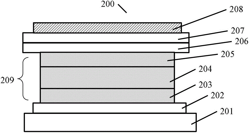
[0068] Figure 2-3 A first embodiment of the invention is shown.

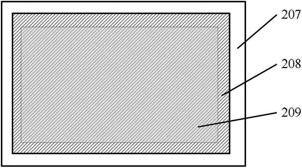
[0069] figure 2 is a schematic structural diagram of the image sensor 200 according to the first embodiment of the present invention, as figure 2 As shown, the image sensor 200 in this embodiment includes: a substrate 201 , a top electrode layer 206 , a common electrode layer 207 , a photodiode structure layer 209 , a bottom electrode layer 202 and an adjustment layer 208 . Wherein, the photodiode structure layer 209 is arranged between the su...


PUM


Abstract

The invention discloses an image sensor, which comprises a substrate and an optical sensor array located on the substrate, wherein the optical sensor array comprises a plurality of scanning lines, a plurality of data lines crossed in an insulation mode with the plurality of scanning lines, and optical sensors and switch units arranged in pixel regions surrounded by adjacent scanning lines and adjacent data lines; and the optical sensor array also comprises optical adjusting layers arranged on the optical sensors for adjusting photoelectric conversion efficiency of the optical sensors. According to the image sensor, the existing image sensor is improved, and adjustability of the photoelectric conversion efficiency is realized.

Description

technical field [0001] The invention relates to a device for photoelectric conversion, in particular to an image sensor. Background technique [0002] A photodiode is a component that absorbs a light signal-photon (Photon) and converts it into an electrical signal-current, usually called Photo-Diode (PD) in English. Such as figure 1 As shown, the PIN junction diode is the most commonly used type of silicon photodiode because it consists of three layers, namely p-type silicon layer (P layer) 101, intrinsic (intrinsic) silicon layer (I layer) 102 and n-type silicon layer (N layer) 103, so it is called a silicon photodiode with PIN junction. PIN junction diodes have the characteristics of fast response speed, low dark current and high sensitivity from the ultraviolet to the near infrared region. It can be used in fields such as photodetectors and optical communications. [0003] An important use of photodiodes is to form arrays for image sensing. Image sensors are currentl...

Claims


Application Information

Patent Timeline
Patent Type & Authority Patents(China)
IPC IPC(8): H01L27/146
Inventor 凌严
Owner SHANGHAI TIANMA MICRO ELECTRONICS CO LTD
Why Eureka
Try Eureka