Polarity face GaN-based light-emitting device capable of improving light-emitting efficiency

A light-emitting device, GaN-based technology, applied in semiconductor devices, electrical components, circuits, etc., can solve problems such as interface conduction band downshift, positive and negative charge center asymmetry, unfavorable electron leakage, etc.

Active Publication Date: 2014-06-25
INST OF SEMICONDUCTORS - CHINESE ACAD OF SCI
View PDF4 Cites 30 Cited by
  • Summary
  • Abstract
  • Description
  • Claims
  • Application Information

AI Technical Summary

Problems solved by technology

However, at present, the composition materials of GaN-based light-emitting devices are generally wurtzite structures grown along the Ga plane (the Ga plane is on the top and the N plane is on the bottom, that is, the c-plane along the growth direction). The positive and negative charge centers are asymmetrical, and there are polar Due to the polarization effect, positive polarization charges will be formed at the interface of AlxGa1-xNLQB / AlyGa1-yN EBL (0≤x
At the same time, the valence band moves up, forming a potential barrier to holes, making hole injection more insufficient, and insufficient hole injection will induce greater electron leakage.

Method used


Image

  • Polarity face GaN-based light-emitting device capable of improving light-emitting efficiency
  • Polarity face GaN-based light-emitting device capable of improving light-emitting efficiency
  • Polarity face GaN-based light-emitting device capable of improving light-emitting efficiency

Examples


Embodiment Construction

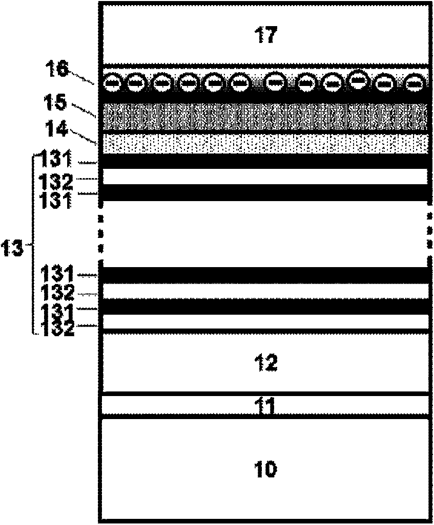
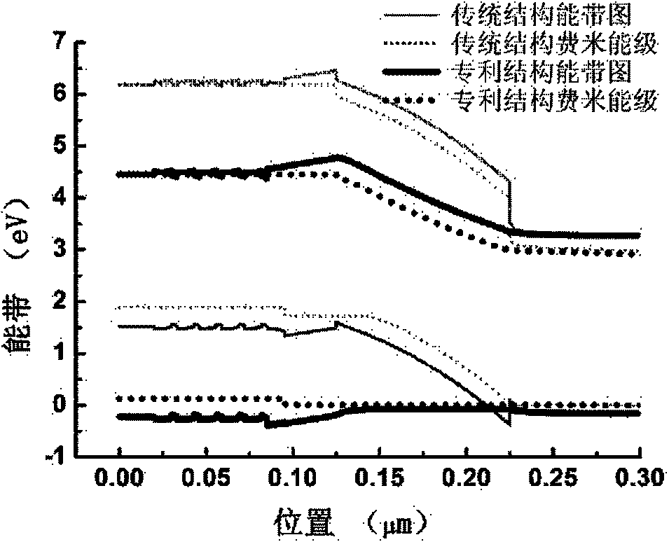
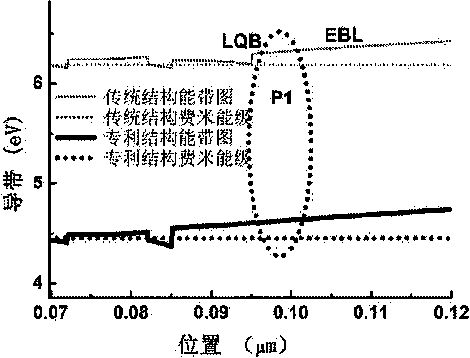
[0015] refer to figure 1 As shown, this embodiment provides an AlGaN DUV LED with a light emission wavelength of about 280nm using the structure of this patent, which includes:

[0016] A substrate 10; the substrate 10 is a (0001) crystal orientation (ie c-plane) sapphire substrate; it can also be GaN, 6H-SiC, 4H-SiC, Si, AlN or ZnO;

[0017] A buffer layer 11, which is made on the substrate 10; the buffer layer 11 is AlN;

[0018] - n-type Al u Ga 1-u N contact layer 12, it is made on buffer layer 11; Wherein n-type Al u Ga 1-u The range of the Al composition u in the N contact layer 12 is 0.40.6, the doped donor impurity is silicon, and the silicon doping concentration is 10 17 10 19 / cm 3 ;

[0019] A light-emitting active region 13, which is fabricated on n-type Al u Ga 1-u On the N contact layer 12; the luminescent active region 13 is a multi-period structure, each period includes a quantum barrier layer 132 and a quantum well layer 131, and the number of period...


PUM


Abstract

A polarity face GaN-based light-emitting device capable of improving the light-emitting efficiency sequentially comprises a substrate, a buffering layer, an n-type AluGal-uN contact layer, a light-emitting active region, a last AlxGal-xN quantum barrier layer, an AlyGal-yN electron barrier layer, an Al component gradual-change AlGaN layer and a p-type AlzGal-zN contact layer, wherein 0<=u, x, y, z <= 1. The polarity face GaN-based light-emitting device is characterized in that an Al component x in the last AlxGal-xN quantum barrier layer is identical to an Al component y in the AlyGal-yN electron barrier layer. According to the polarity face GaN-based light-emitting device, the electron blocking effect is improved and hole injection is improved so that electron leakage can be effectively reduced, and therefore the light-emitting efficiency of the device is improved.

Description

technical field [0001] The invention belongs to the technical field of semiconductors, and in particular refers to a gallium nitride-based polar surface light-emitting device with improved luminous efficiency, which is suitable for gallium nitride-based ultraviolet, blue or green light-emitting devices prepared with polar surface materials, and is A light-emitting device structure that improves luminous efficiency by increasing electron blocking effect and improving hole injection through energy band regulation and polarization regulation, especially more effective for deep ultraviolet light-emitting diodes. Background technique [0002] Semiconductor lighting centered on gallium nitride (GaN)-based light-emitting diodes (LEDs) has experienced exceptionally rapid development in recent years. According to reports, lighting electricity consumption accounts for about 20% of the entire electricity consumption. The efficiency of incandescent lamps for traditional lighting is ver...

Claims


Application Information

Patent Timeline
Patent Type & Authority Applications(China)
IPC IPC(8): H01L33/14H01L33/06
CPCH01L33/06H01L33/14H01L33/32
Inventor 姬小利闫建昌郭金霞张连杨富华段瑞飞王军喜曾一平王国宏李晋闽
Owner INST OF SEMICONDUCTORS - CHINESE ACAD OF SCI
Why Eureka
Try Eureka