Method for making thick copper printed circuit board

A technology of copper printed circuit board and manufacturing method, which is applied in the direction of removing conductive materials by chemical/electrolytic methods, can solve the problems of too thick surface copper, inability to form patterns, etching, and lamination, and achieves high alignment accuracy. Effect

Inactive Publication Date: 2014-06-25
JIUJIANG HUAXIANG TECH +2
View PDF5 Cites 6 Cited by
  • Summary
  • Abstract
  • Description
  • Claims
  • Application Information

AI Technical Summary

Problems solved by technology

In the subsequent graphics process, a photosensitive dry film should be covered on the copper layer. Too thick surface copper will wrap the photosensitive dry film, resulting in the inability to form graphics and etching, resulting in the so-called "clamp film" problem.
[0004] On the other hand, too thick surface copper will also make subsequent etching difficult, or the wires of the PCB circuit board will be too thin after multiple etchings.

Method used


Image

  • Method for making thick copper printed circuit board

Examples


Embodiment Construction

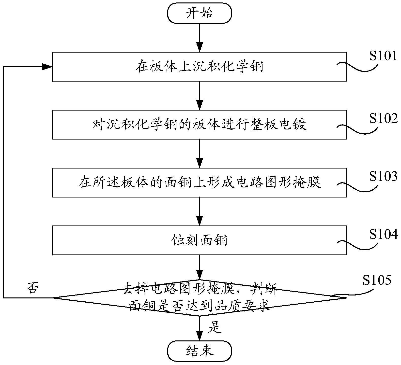
[0027] Such as figure 1 Shown is a flowchart of a method for manufacturing a thick copper printed circuit board according to an embodiment. The method comprises the steps of:

[0028] Step S101: Depositing chemical copper on the board body. This step is referred to as copper sinking for short, and is to deposit a thin layer of chemical copper on the board body by chemical method, as the base of electroplating copper later. Its main process includes: alkaline degreasing → secondary or tertiary countercurrent rinsing → coarsening (micro-etching) → secondary countercurrent rinsing → presoaking → activation → secondary countercurrent rinsing → degumming → secondary countercurrent rinsing → sinking Copper → secondary countercurrent rinsing → pickling. The copper sinking process is a standard process for making printed circuit boards. There may be some differences for different requirements, and the specific steps will not be repeated.

[0029] Step S102: Electroplating the enti...


PUM


Abstract

The invention discloses a method for making a thick copper printed circuit board. The method comprises the following steps of (A) depositing chemical copper on a board body, (B) carrying out whole board plating on the board body where the chemical copper is deposited, (C) forming a circuit pattern mask on the surface copper of the board body, (D) etching the surface copper, and repeating the steps of (A), (B), (C) and (D) until the surface copper reaches the requirement of quality. According to the above method for making the thick copper printed circuit board, a circuit pattern is thickened gradually through the processes of repeated copper deposition, copper plating and etching, and problems of 'film clipping' and too thin conductive wire brought by the direct etching on the thick copper board can be effectively avoided.

Description

technical field [0001] The invention relates to a printed circuit board technology, in particular to a method for manufacturing a thick copper printed circuit board. Background technique [0002] In the production of PCB thick copper plate, the traditional production method is to deposit the copper layer on the PCB body, then electroplate the surface copper to meet the quality requirements at one time, and then use repeated etching to obtain the required graphic circuit. The basic process is: deposition of copper layer → electroplating of the whole board → formation of graphics → electroplating graphics → multiple etching. [0003] In the above process, since it is a thick copper board PCB, the deposited copper layer plus the copper layer plated on the entire board will form a very thick surface copper. In the subsequent graphics process, a photosensitive dry film needs to be covered on the copper layer. Excessively thick surface copper will wrap the photosensitive dry film...

Claims


Application Information

Patent Timeline
Patent Type & Authority Applications(China)
IPC IPC(8): H05K3/06
Inventor 姚国庆钟文超
Owner JIUJIANG HUAXIANG TECH
Why Eureka
Try Eureka