

Method for preparing graphene fine wires
A fine circuit and graphene technology, which can be applied to the formation of conductive patterns and other directions, can solve problems such as the preparation method of graphene-free fine circuits, and achieve the effects of low cost and simple and controllable method.
- Summary
- Abstract
- Description
- Claims
- Application Information
AI Technical Summary
Problems solved by technology
Method used
Image

Examples
preparation example Construction
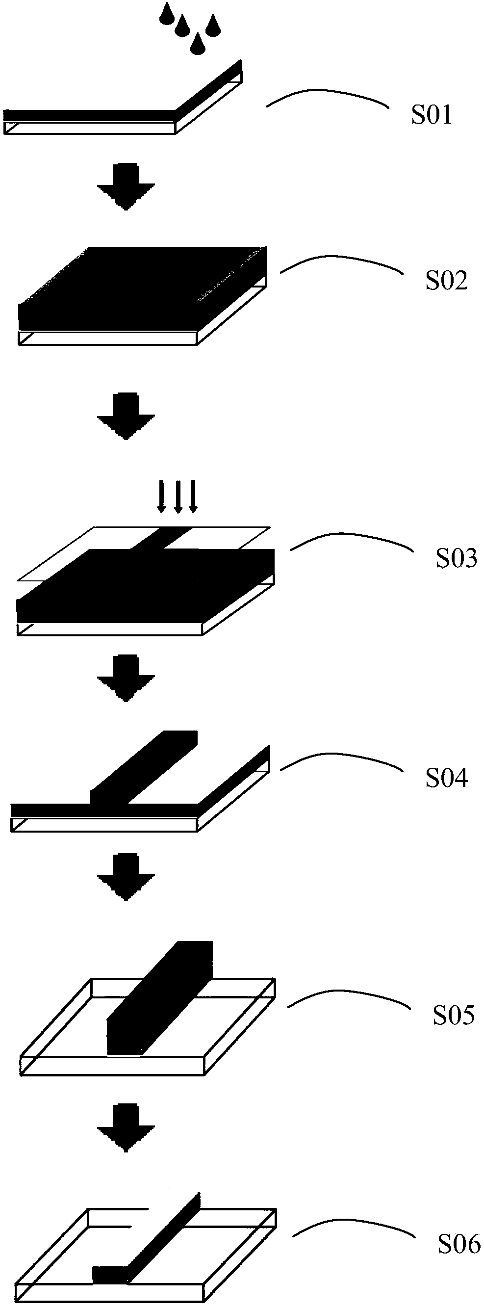
[0017] The embodiment of the present invention provides a method for preparing graphene fine circuit, comprising the following steps, specifically as attached figure 1 Shown:
[0018] S01. Cleaning: coating a layer of graphene film on the carrier substrate, and cleaning the surface of the graphene film;
[0019] S02. Coating: coating a layer of photoresist on the surface of the cleaned graphene film to form a photoresist layer;
[0020] S03. Exposure: Position and install a photomask parallel to the photoresist layer above the surface of the photoresist layer and designed with a sample pattern template, and perform exposure treatment on the photoresist layer with the above photomask installed, wherein, The size ratio of the sample drawing template to the physical circuit is 1:1;
[0021] S04. Developing: immerse the exposed sample in a developing solution for developing, and remove the exposed photoresist;
[0022] S05. Etching: placing the sample after the above-mentioned ...
Embodiment 1
[0048] A preparation method for producing fine lines of liquid crystal display screens from graphene, comprising the following steps:
[0049] S11. Cleaning: coating a layer of graphene film on the glass substrate, the thickness of the graphene film is 0.05nm, cleaning the surface of the graphene film, the cleaning is sequentially soaked in 0.5mol / L KOH solution 2.5 hours, rinsing with pure water, scrubbing, ultrasonic treatment with pure water, and drying, the drying temperature of the drying treatment is 110°C;
[0050] S12. Coating: coating a layer of positive photoresist on the surface of the cleaned graphene film to form a photoresist layer, the ratio of weight and number of photosensitive agent, resin, sensitizer and solvent in the photoresist is preferred It is 5:20:1:70, the volume ratio of photoresist and diluent in the coating process is 10:1, and the photoresist concentration after dilution is 5ppm;
[0051] S13. Exposure: Position and install a photomask on the su...
Embodiment 2
[0056] A preparation method for producing fine circuits of electronic chips from graphene, comprising the following steps:
[0057] S21. Cleaning: coating a layer of graphene film on the glass substrate, the thickness of the graphene film is 0.03nm, cleaning the surface of the graphene film, the cleaning is sequentially soaked in 0.6mol / L KOH solution 2 hours, rinsing with pure water, scrubbing, ultrasonic treatment with pure water, and drying, the drying temperature of the drying treatment is 120°C;
[0058]S22. Coating: coating a layer of positive photoresist on the surface of the cleaned graphene film to form a photoresist layer, the photoresist, resin, sensitizer and solvent in the photoresist The weight and number ratio is preferred 5:15:0.8:65, the volume ratio of the photoresist and diluent in the coating process is 9:1, and the diluted photoresist concentration is 8ppm;
[0059] S23. Exposure: Position and install a photomask that is completely parallel to the photore...
PUM
| Property | Measurement | Unit |
|---|---|---|
| thickness | aaaaa | aaaaa |
| electrical resistivity | aaaaa | aaaaa |
| thickness | aaaaa | aaaaa |
Abstract
Description
Claims
Application Information