

Semiconductor integrated circuit device
A technology of integrated circuits and semiconductors, applied in the manufacture of semiconductor devices, circuits, semiconductor/solid-state devices, etc., can solve the problems of increased area and large cell width, and achieve the effect of improving the driving ability
- Summary
- Abstract
- Description
- Claims
- Application Information
AI Technical Summary
Problems solved by technology
Method used
Image

Examples
no. 1 approach
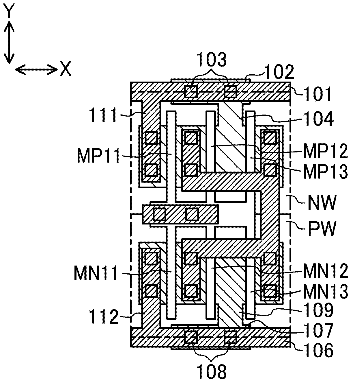
[0050] figure 1 It is a plan view showing the layout structure of the single height cell in the first embodiment. A single-height unit is a unit that has the height of a base unit. exist figure 1 In , the dotted line represents the unit box. In addition, the horizontal direction (X direction) of a drawing is a cell width direction, and the vertical direction (Y direction) of a drawing is a cell height direction (it is the same for the following drawings).
[0051] exist figure 1 Among them, MP11-MP13 are PMOS transistors formed in N-well NW, and MN11-MN13 are NMOS transistors formed in P-well PW. 101 is a power wiring, and 106 is a ground wiring, both of which are formed on the first metal wiring layer. The power supply wiring 101 and the ground wiring 106 are respectively arranged at both ends in the cell height direction of the single-height cell so as to extend from the right end to the left end of the cell frame in the cell width direction. The centerline of the p...
no. 2 approach
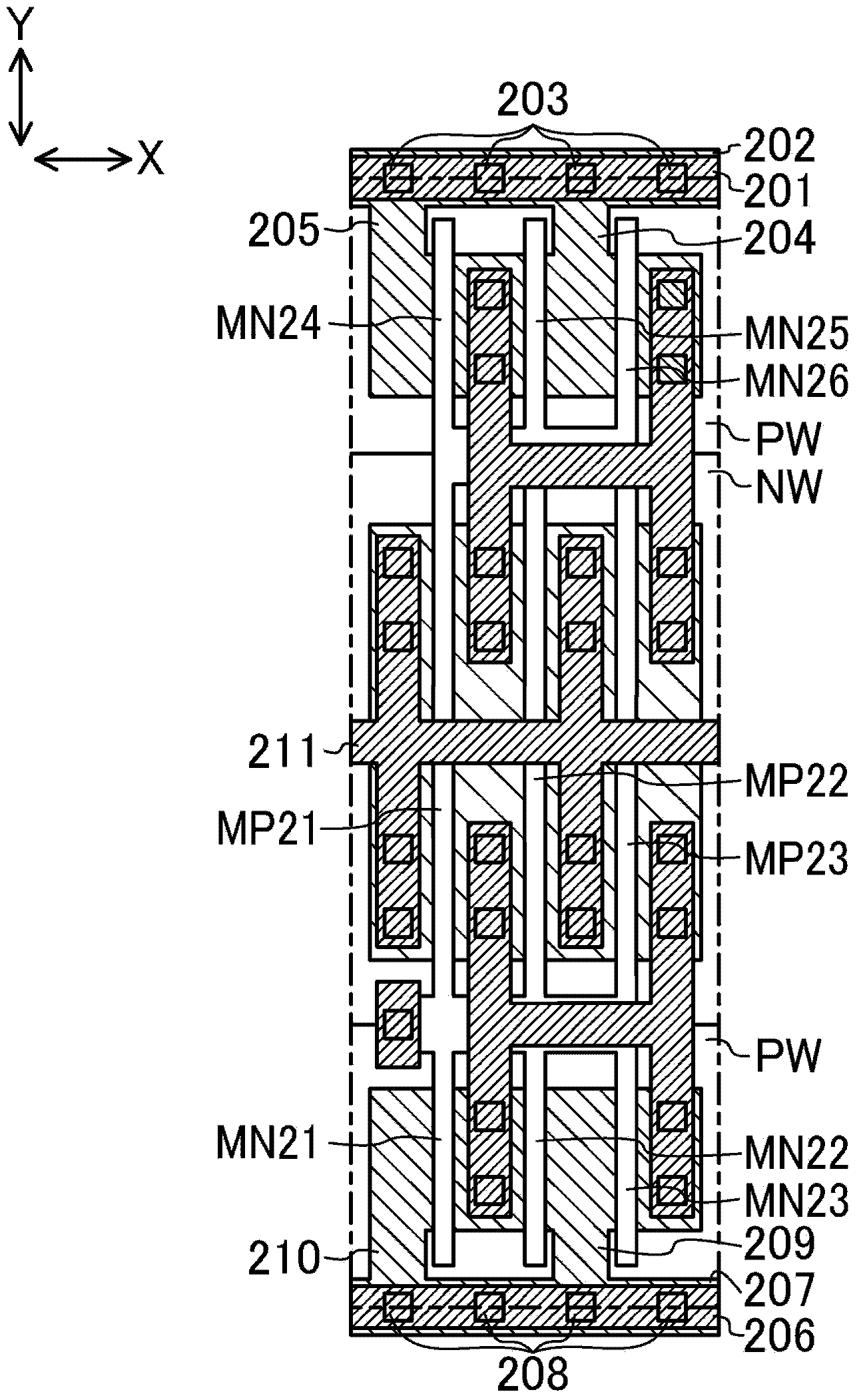
[0063] Figure 4 It is a plan view showing the layout structure of the single-height cell in the second embodiment. exist Figure 4 in, right with figure 1 The same constituent elements are labeled with figure 1 The same reference numerals are used, and detailed descriptions thereof are omitted here.
[0064] Figure 4 The layout structure of the figure 1 In substantially the same way, the P+ diffusion wiring 102 and the N+ diffusion wiring 107 are arranged at predetermined intervals from the left and right ends of the cell frame in the cell width direction. However, the specified interval is figure 1 different. exist Figure 4Among them, the P+ diffusion wiring 102 and the N+ diffusion wiring 107 are arranged at intervals of 1 / 2SP from the left and right ends of the cell frame. In addition, the positions of the contact 103 connecting the P+ diffusion wiring 102 to the power supply wiring 101 and the contact 108 connecting the N+ diffusion wiring 107 to the ground...
no. 3 approach
[0082] Figure 9 It is a diagram showing a part of the design flow of the semiconductor integrated circuit device according to the third embodiment. exist Figure 9 Among them, S11 is a layout design step in which arrangement of standard cells, wiring between standard cells, etc. are performed, and layout design data is created. Here, the standard cells are arranged based on the cell frame. S12 is a layer calculation processing step in which a layout change is performed on the layout design data created in the layout design step S12 in consideration of overlapping layers for calculation. In addition, the calculation layer is a concept on the design data for modifying the layout, and does not appear in the actual layout structure. S13 is a layout inspection step, in which design rules and the like are inspected for the layout data LD1 after the arithmetic processing.
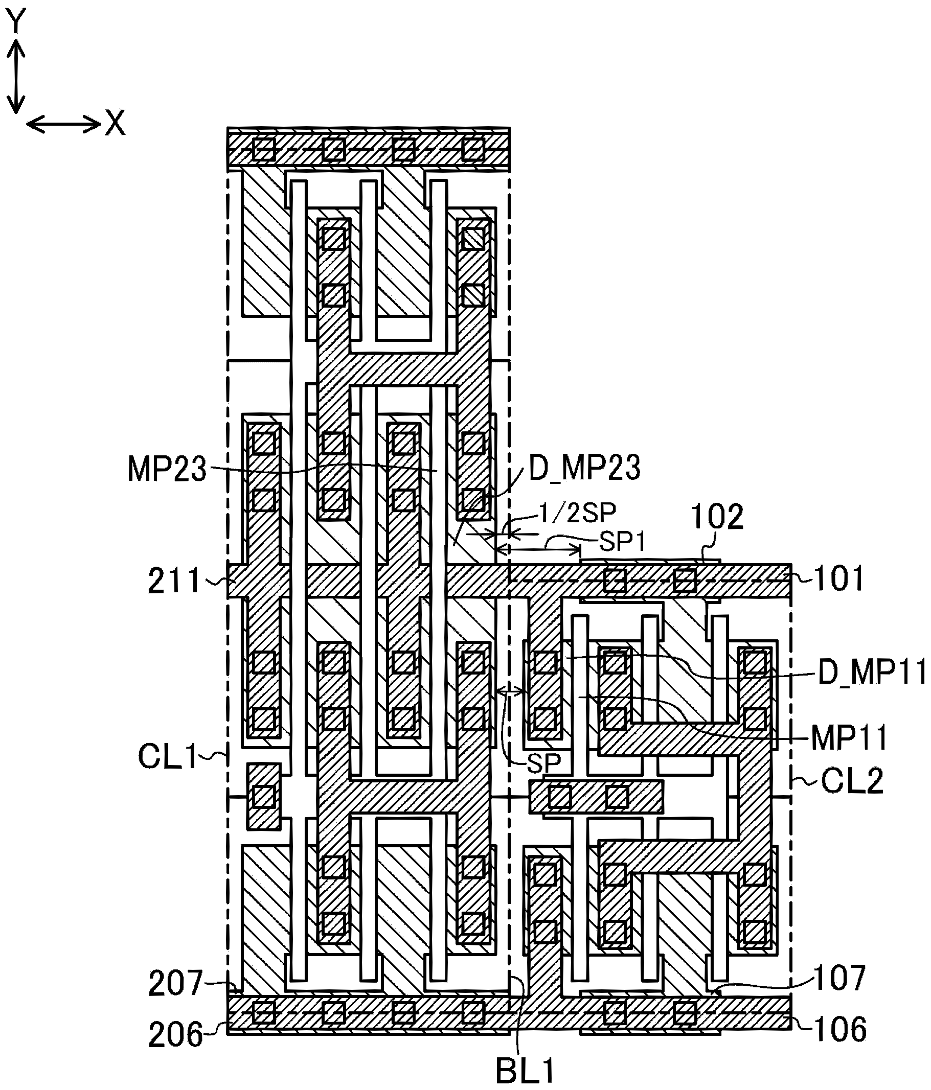
[0083] Figure 10 It is a figure which shows the design data of the single-height unit of this embodiment...
PUM
 Abstract
Description
Claims
Application Information