Silicon wafer transfer device

A handover device and silicon wafer technology, which is applied in the direction of exposure device, transportation and packaging, conveyor objects, etc. in the photolithographic process, can solve hidden dangers and safety problems, achieve low cost, simple structure, and eliminate potential safety hazards.

Active Publication Date: 2014-07-02
SHANGHAI MICRO ELECTRONICS EQUIP (GRP) CO LTD
View PDF5 Cites 6 Cited by
  • Summary
  • Abstract
  • Description
  • Claims
  • Application Information

AI Technical Summary

Problems solved by technology

[0004] The invention provides a silicon chip handover device to overcome the problem of safety hazards in the silicon chip handover process in the prior art

Method used


Image

  • Silicon wafer transfer device
  • Silicon wafer transfer device
  • Silicon wafer transfer device

Examples


Embodiment 1

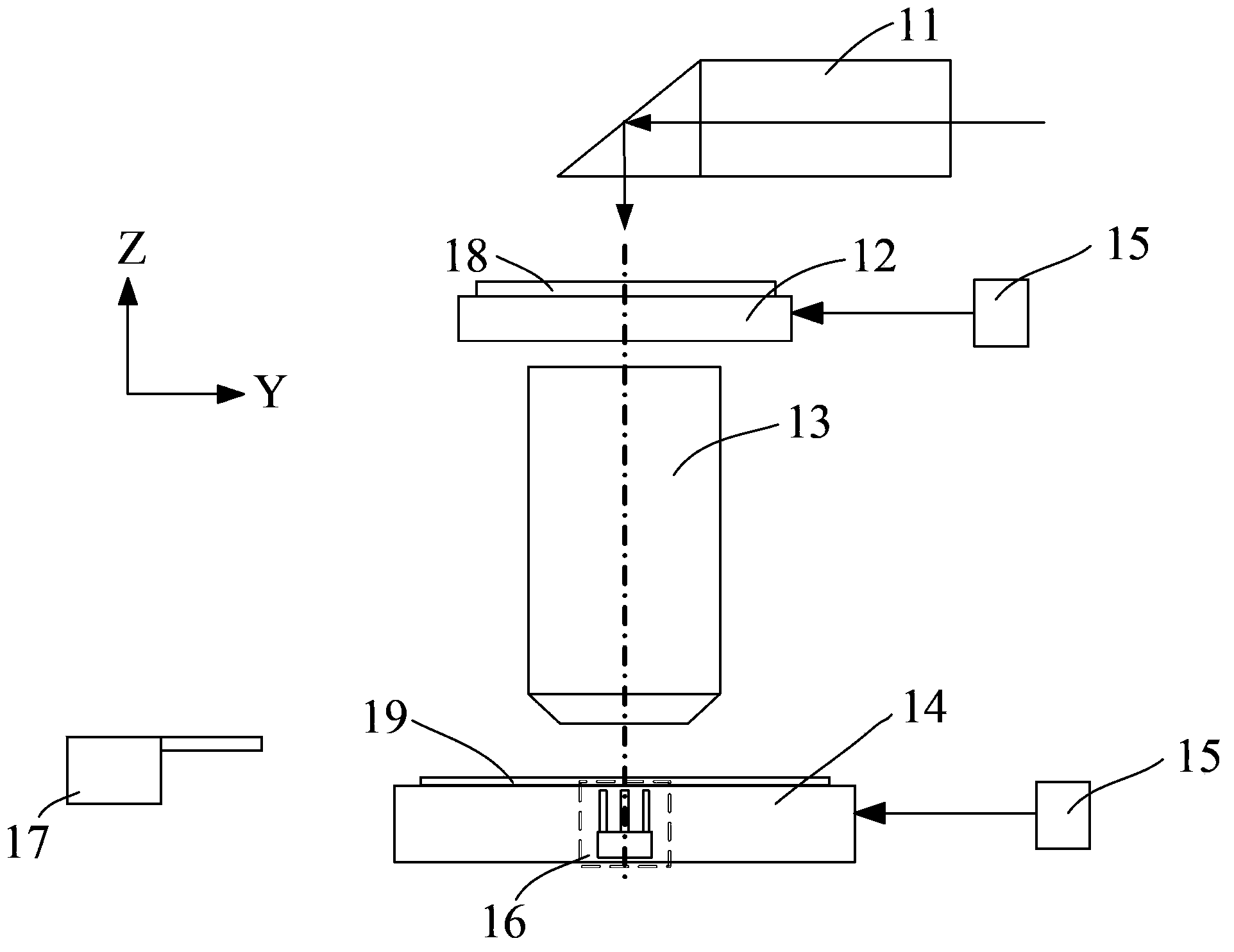
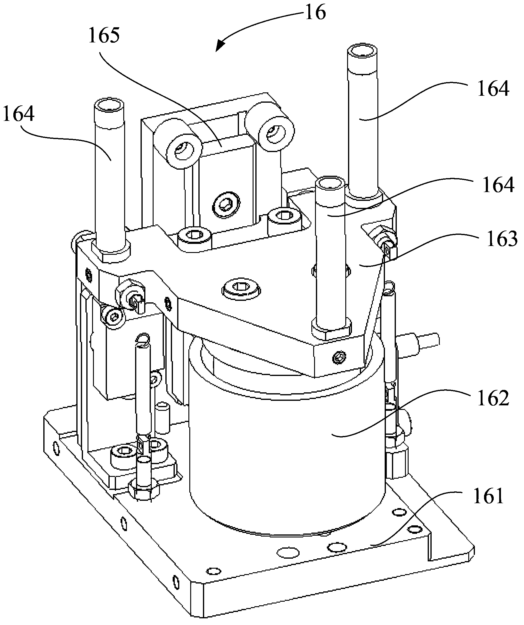
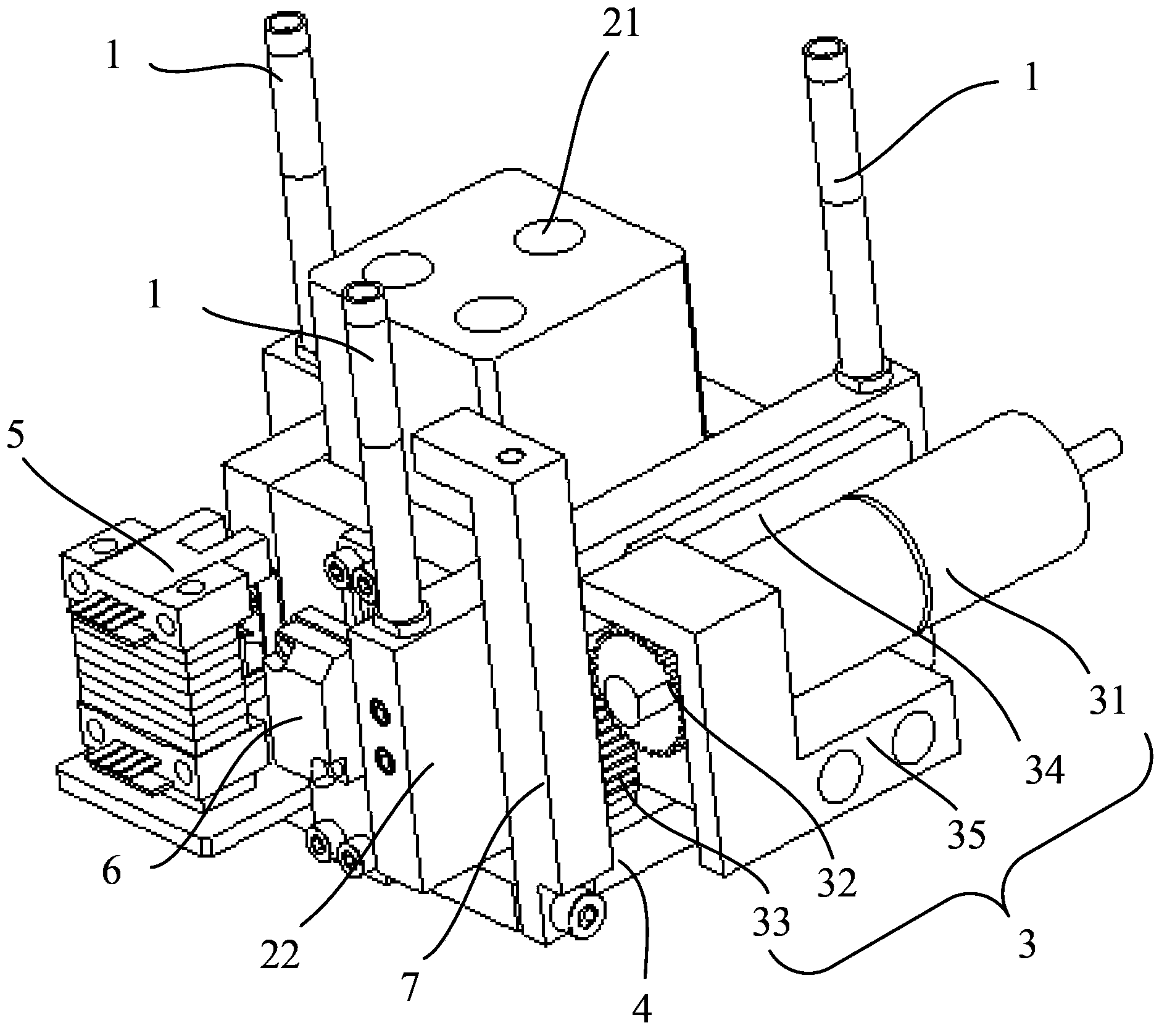
[0037] Please refer to image 3 , and combined with Figure 4~5 , the silicon wafer handover device of this embodiment includes a hand 1 , an air bearing rail device 2 , a driving mechanism 3 and a base 4 . Wherein, the splicing hand 1 is fixed on the top of the air-floating guide rail device 2, the air-floating guide rail device 2 and the driving mechanism 3 are fixed on the base 4, and the driving mechanism 3 drives the air-floating guiding rail Device 2 moves. Specifically, the splicing hand 1 is used for absorbing silicon wafers and providing a supporting surface for the silicon wafers; The splicing hand 1; the driving mechanism 3 provides the driving force for the vertical movement of the silicon wafer handover device, and provides a frictionless linear guide function for the vertical movement of the silicon wafer handover device. Therefore, the silicon wafer transfer device in this embodiment solves the friction problem of the guide mechanism in the prior art. At the ...

Embodiment 2

[0052] The difference between this embodiment and Embodiment 1 lies in the structural shape of the air-floating guide rail device.

[0053] Please refer to Figure 6 , in this embodiment, the air-floating rail device 2' includes an air-floating rail stator 21' and an air-floating rail mover 22', wherein the air-floating rail stator 21' is a prism, and the air-floating rail mover 22' It is a hollow prism or cuboid, and the shape of the hollow part corresponds to the shape of the air bearing guide rail stator 21'. Similarly, the air-floating guide rail device 2' in this embodiment can effectively prevent deflection between the air-floating guide rail movable stator 21' and the air-floating guide rail mover 22', avoiding damage to the silicon wafer or the upper surface of the splicing hand. If it is not parallel to the base, it will affect the subsequent photolithography process.

Embodiment 3

[0055] The difference between this embodiment and Embodiment 1 and Embodiment 2 is that the structure and shape of the air-floating guide rail device and its airflow channel are different.

[0056] Please refer to Figure 7 , in this embodiment, the air-floating rail device 2" includes an air-floating rail stator 21" and an air-floating rail mover 23", the air-floating rail stator 21" is a cylinder, and the air-floating rail mover 23" It is a cylinder or a cuboid, and the shape of the hollow part corresponds to the shape of the air bearing guide rail stator 21". Preferably, an anti-deflection device 22" is provided between the air-floating guide rail mover 23" and the air-floating guide rail stator 21", so as to prevent the air-floating guide rail stator 21" from contacting the air-floating guide rail mover. 23" deflection. Similarly, the air-floating guide rail device 2" can effectively prevent deflection between the air-floating guide rail movable stator 21" and the air-flo...


PUM

PropertyMeasurementUnit
diameteraaaaaaaaaa
widthaaaaaaaaaa
depthaaaaaaaaaa

Abstract

The invention discloses a silicon wafer transfer device. The silicon wafer transfer device comprises a wafer receiving manipulator, an air flotation guide rail device, a driving mechanism and a base, wherein the air flotation guide rail device comprises an air flotation guide rail stator and an air flotation guide rail rotator, the air flotation guide rail stator is fixed on the base, the air flotation guide rail rotator is arranged on the air flotation guide rail stator in a sleeving manner and is fixedly connected with the wafer receiving manipulator, and the driving mechanism drives an air flotation guide rail device to move. The silicon wafer transfer device disclosed by the invention solves the problem of friction of a guide mechanism in the prior art by adopting the air flotation guide rail device, ensures that the wafer receiving manipulator can return to the lowest position after a silicon wafer is transferred, and eliminates the potential safety hazard as the wafer receiving manipulator cannot return to the lowest position in silicon wafer transferring in the prior art, meanwhile the entire structure is simple, and the cost is low.

Description

technical field [0001] The invention relates to the field of photolithography equipment, in particular to a silicon wafer transfer device. Background technique [0002] The photolithography apparatus in the prior art is mainly used in the manufacture of integrated circuits IC, flat panel display fields or other micro devices. With a photolithographic apparatus, multilayer masks with different mask patterns are sequentially imaged in precise alignment on a photoresist-coated wafer, such as a semiconductor wafer or an LCD panel. Please refer to figure 1 , is a structural schematic diagram of an existing lithography apparatus, ie, a lithography machine. From figure 1 It can be seen from the figure that the lithography machine includes: an illumination system 11 , a mask table 12 , a projection objective lens 13 , a workpiece table 14 , a laser interferometer 15 , a wafer transfer device 16 and a transmission system 17 . Among them, the illumination system 11 provides the ex...

Claims


Application Information

Patent Timeline
Patent Type & Authority Applications(China)
IPC IPC(8): G03F7/20H01L21/677
Inventor 梁晓叶江旭初
Owner SHANGHAI MICRO ELECTRONICS EQUIP (GRP) CO LTD
Why Eureka
Try Eureka