Gate oxide failure point positioning method

A technology of gate oxide layer and positioning method, which is applied in semiconductor/solid-state device testing/measurement, material analysis by measuring secondary emissions, etc., and can solve positioning dependence, poor positioning accuracy, and success rate of gate oxide layer failure analysis efficiency Low-level problems, to achieve the effect of improving efficiency, improving success rate, and shortening preparation time

Active Publication Date: 2014-07-16
WUHAN XINXIN SEMICON MFG CO LTD
View PDF10 Cites 20 Cited by
  • Summary
  • Abstract
  • Description
  • Claims
  • Application Information

AI Technical Summary

Problems solved by technology

[0015] In view of the above existing problems, the present invention discloses a method for locating the failure point of the gate oxide layer, so as to overcome the fact that the location of the failure point of the ga

Method used


Image

  • Gate oxide failure point positioning method
  • Gate oxide failure point positioning method
  • Gate oxide failure point positioning method

Examples


Embodiment Construction

[0044] The present invention will be further described below in conjunction with the accompanying drawings and specific embodiments, but not as a limitation of the present invention.

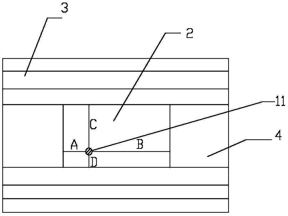
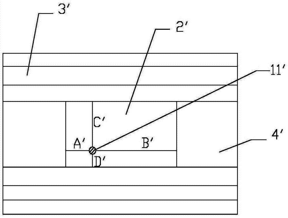
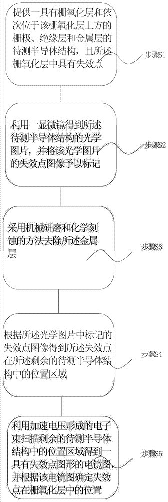
[0045] figure 1 is a schematic diagram of the optical map that uses color to mark the breakdown point of the gate oxide layer, image 3 is a schematic flowchart of a method for locating failure points of a gate oxide layer in an embodiment of the present invention, Figure 4-6 Respectively, in the embodiment of the present invention, a scanning electron microscope detector is used to scan the electron beam formed under the acceleration voltage of 4KV, 10KV, and 20KV to scan the semiconductor structure to be tested after removing the metal layer. Figure 7 It is a schematic diagram of the principle that the electron beam scanning formed by the scanning electron microscope detector under the medium-high speed accelerating voltage can locate the breakdown point in the embodiment of the present inv...


PUM


Abstract

The invention discloses a gate oxide failure point positioning method. after removal of a metal layer, a semiconductor structure to be measured obtained after removal of the metal layer is scanned by the use of an electron beam formed by medium and high accelerating voltage so as to obtain an electron microscope with a failure point pattern; and according to the electron microscope, the position of the failure point in a gate oxide is determined so as to more precisely position a breakdown point of the gate oxide. Furthermore, success rate of gate oxide breakdown voltage test failure analysis is raised effectively; preparation time of a follow-up transmission electron microscope sample is further shortened; efficiency of gate oxide breakdown voltage test failure analysis is raised; and necessary conditions are provided for the preparation of the transmission electron microscope sample which requires precise positioning. In addition, the breakdown point of the gate oxide and failure analysis of the gate oxide can still be positioned precisely when an optical positioning machine cannot be used.

Description

technical field [0001] The invention relates to the technical field of semiconductor manufacturing, in particular to a method for locating failure points of gate oxide layers. Background technique [0002] With the continuous shrinking of the size of integrated circuits, the quality and reliability of the gate oxide (GOX) of semiconductor devices becomes more and more important. However, due to the reduction of the size of semiconductor devices, there are The failure point becomes more and more difficult. [0003] The gate oxide breakdown voltage test (GOI V-ramp) is a common method to evaluate the quality of the gate oxide layer, and the gate oxide breakdown voltage test structure is generally very large (thousands, or even tens of thousands of square microns), so The location of the gate oxide breakdown point (also known as the failure point) is particularly important in the failure analysis of the gate oxide breakdown voltage test as a prerequisite for physical failure a...

Claims


Application Information

Patent Timeline
IPC IPC(8): G01N23/22H01L21/66
Inventor 李桂花仝金雨刘君芳郭伟李剑
Owner WUHAN XINXIN SEMICON MFG CO LTD
Why Eureka
Try Eureka