Organic electroluminescence device, and manufacturing method and display device thereof

An electroluminescence device and a luminescence technology, which are applied in the manufacture of organic semiconductor devices, electric solid devices, semiconductor/solid state devices, etc., can solve problems such as inability to extract and emit light beams, increase beam reflection or total reflection, etc.

Active Publication Date: 2014-07-16
BOE TECH GRP CO LTD
View PDF8 Cites 18 Cited by
  • Summary
  • Abstract
  • Description
  • Claims
  • Application Information

AI Technical Summary

Problems solved by technology

[0004] However, when applying the above-mentioned patents, it was found that the direction of the received beam would be changed due to the nanoparticle layer on the substrate would scatter the beam. The possibility

Method used


Image

  • Organic electroluminescence device, and manufacturing method and display device thereof
  • Organic electroluminescence device, and manufacturing method and display device thereof

Examples


preparation example Construction

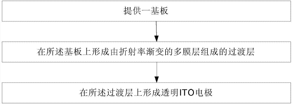
[0044] Another aspect of the present invention also provides a method for preparing an organic electroluminescent device comprising any of the above embodiments, such as figure 2 shown, including:

[0045] 21: Provide a substrate.

[0046] In this step, the substrate may be a glass substrate. It can be understood that the substrate can also be selected from plastic substrates, and it can be further understood that since the refractive index of the plastic substrate is between 1.5-1.65, when the substrate is selected from a plastic substrate, the corresponding bonding is low. The material of the refractive index film layer also needs to be adjusted accordingly to meet the needs of adjusting the refractive index.

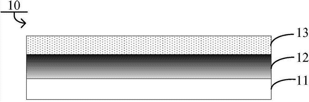
[0047] 22: Forming a transition layer composed of multilayer film layers with graded refractive index on the substrate.

[0048] In this step, four small steps can be further included, specifically:

[0049] 1): Mix materials with high and low refractive indices ...

Embodiment 1

[0063] 1) Select polyimide with rigid structure (refractive index greater than 1.8) as high refractive index material, choose flexible polysiloxane (refractive index less than 1.4) as low refractive index material, use tetrahydrofuran and N,N-two Methylacetamide was used as a mixed solvent. Dissolve the above polyimide and polysiloxane in a mixed solvent of tetrahydrofuran and N,N-dimethylacetamide (volume ratio 1:1) according to 50:50wt%, and then put the above mixed solution at room temperature (20°C) and spin-coated on the substrate to form a thin film layer with uniform thickness.

[0064] 2) Utilize the good solubility of polysiloxane in tetrahydrofuran, but the poor solubility in N,N-dimethylacetamide; at the same time, polyimide has good solubility in N,N-dimethylacetamide, Characterized by poor solubility in THF, control the solvent evaporation temperature of the spin-coated film, such as at room temperature (20°C), for phase separation of polyimide and polysiloxane. ...

Embodiment 2

[0069] 1) Select fluorinated polyimide (refractive index greater than 1.8) with rigid structure as high refractive index material, choose flexible polypropylene oxide (refractive index less than 1.4) as low refractive index material, and fluorinated polyimide Amine and polypropylene oxide 60:40wt% are dissolved in an organic solvent, such as dimethyl sulfoxide, and the above organic solution is slit-coated to form a thin film layer with uniform thickness on the surface of the substrate.

[0070] 2) Low-temperature annealing is used to remove the organic solvent (temperature below 100°C) to form an organic dry film. Since the glass transition temperature of fluorinated polyimide is higher than 250°C, the glass transition temperature of polypropylene oxide is lower than 180°C. Utilizing the different glass transition temperatures of the two polymers, the high-temperature annealing temperature was selected to be 200°C (higher than the glass transition temperature of polypropylene...


PUM


Abstract

The embodiment of the invention provides an organic electroluminescence device, and a manufacturing method and a display device of the organic electroluminescence device, and belongs to the field of organic electroluminescence devices. The organic electroluminescence device enhances the light emitting efficiency of devices, and comprises a substrate, a transition layer and a transparent ITO electrode, wherein the substrate, the transition layer and the transparent ITO electrode are sequentially arranged. The transition layer is composed of a plurality of film layers with the gradually-changed refractive indexes, the refractive indexes are gradually increased from bottom to top in the direction perpendicular to the substrate, the refractive index of the film layer, close to the transparent ITO electrode, of the transition layer is larger than or equal to the refractive index of the transparent ITO electrode, and the refractive index of the film layer, close to the substrate, of the transition layer is smaller than or equal to the refractive index of the substrate. The manufacturing method and the display device of the organic electroluminescence device can be used in manufacturing of the organic electroluminescence device.

Description

technical field [0001] The invention relates to the field of organic electroluminescent devices, in particular to an organic electroluminescent device, a preparation method thereof, and a display device. Background technique [0002] In a traditional organic electroluminescent device, its structure is sequentially provided with a substrate, a transparent ITO electrode, an organic layer and a second electrode layer from bottom to top. Among them, the refractive index of the organic layer is usually 1.7-2.0, the refractive index of the ITO electrode layer is 1.8-1.9, and the refractive index of the glass is about 1.5. The difference in refractive index between the space and the base layer / air produces reflection and total reflection phenomena, so that the light beam has to be confined in the ITO electrode layer or the substrate and cannot be emitted, resulting in the loss of luminescence, thus affecting the efficiency of the external quantum is very low , only 20%. [0003] ...

Claims


Application Information

Patent Timeline
IPC IPC(8): H01L51/52H01L51/56
CPCH10K50/858H10K2102/331
Inventor 侯文军刘则
Owner BOE TECH GRP CO LTD
Why Eureka
Try Eureka