Color filter substrate, manufacturing method thereof and liquid crystal display panel

A color filter substrate, liquid crystal display panel technology, applied in the direction of filters, optics, optical components, etc., can solve the problem that the color filter substrate 3 and the sealant 4 are easy to peel off, the peeling test does not meet the requirements, and the product quality is affected. and other problems, to avoid liquid crystal leakage, change the shape of the contact surface, and improve the quality

Inactive Publication Date: 2014-07-23
WUHAN TIANMA MICRO ELECTRONICS CO LTD
View PDF6 Cites 40 Cited by
  • Summary
  • Abstract
  • Description
  • Claims
  • Application Information

AI Technical Summary

Problems solved by technology

However, the results of the peeling test show that the materials of the common electrode layer 6 or black matrix 8 and the sealant 4 differ greatly, and as the frame of the liquid crystal display becomes narrower and narrower, the sealant 4 and the common electrode layer 6 or black matrix The contact area of ​​8 is getting smaller and smaller, which leads to the smaller and smaller adhesion between the color filter substrate 3 and the frame glue 4, which makes the color filter substrate 3 and the frame glue 4 easy to peel off, resulting in liquid crystal leakage and other problems. The peeling test reached Failure to meet requirements affects product quality and reduces production efficiency

Method used


Image

  • Color filter substrate, manufacturing method thereof and liquid crystal display panel
  • Color filter substrate, manufacturing method thereof and liquid crystal display panel
  • Color filter substrate, manufacturing method thereof and liquid crystal display panel

Examples


Embodiment 1

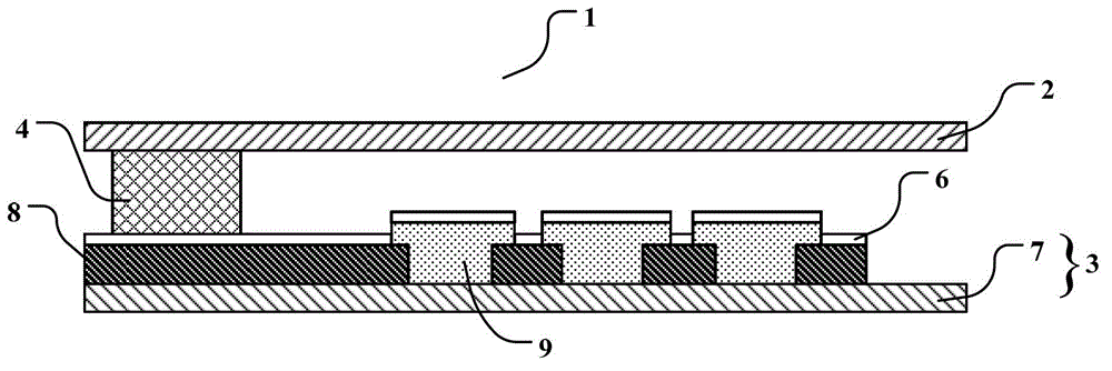
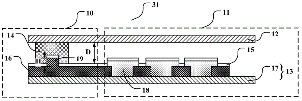
[0028] Please refer to figure 2 , figure 2 It is a partial cross-sectional schematic diagram of a liquid crystal display panel proposed in Embodiment 1 of the present invention, including a color filter substrate with a protrusion formed on the surface of a black matrix in a non-display area. Such as figure 2 As shown, the present invention provides a liquid crystal display panel 31, the liquid crystal display panel 31 has a display area 11 and a non-display area 10 located at the periphery of the display area 11, and the specific structure of the liquid crystal display panel 31 includes: a color filter substrate 13; a thin film transistor array substrate 12, arranged opposite to the color filter substrate 13; a liquid crystal (not shown in the figure), packaged between the color filter substrate 13 and the thin film transistor array substrate 12; also includes A sealant 14 disposed between the thin film transistor array substrate 12 and the color filter substrate 13 in t...

Embodiment 2

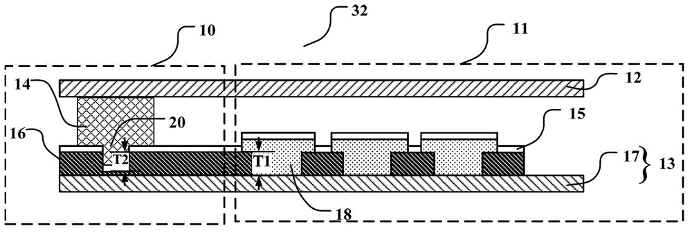
[0035] Please refer to image 3 , image 3 It is a partial cross-sectional schematic diagram of a liquid crystal display panel proposed in Embodiment 2 of the present invention, which includes a color filter substrate with a groove formed on the surface of a black matrix in a non-display area. Such as image 3 As shown, the present invention provides a liquid crystal display panel 32, the liquid crystal display panel 32 has a display area 11 and a non-display area 10 located at the periphery of the display area 11, the specific structure of the liquid crystal display panel 32 includes: a color filter substrate 13; a thin film transistor array substrate 12, arranged opposite to the color filter substrate 13; a liquid crystal (not shown in the figure), packaged between the color filter substrate 13 and the thin film transistor array substrate 12; also includes The sealant 14 is disposed between the thin film transistor array substrate 12 and the color filter substrate 13 in th...

Embodiment 3

[0042] Please refer to Figure 4 , Figure 4 It is a partial cross-sectional schematic diagram of a liquid crystal display panel proposed in Embodiment 3 of the present invention, which includes a color filter substrate with a plurality of protrusions formed on the surface of a black matrix in a non-display area. Such as Figure 4 As shown, the present invention provides a liquid crystal display panel 33, the liquid crystal display panel 33 has a display area 11 and a non-display area 10 located at the periphery of the display area 11, and the specific structure of the liquid crystal display panel 33 includes: a color filter substrate 13; a thin film transistor array substrate 12, arranged opposite to the color filter substrate 13; a liquid crystal (not shown in the figure), packaged between the color filter substrate 13 and the thin film transistor array substrate 12; also includes A sealant 14 disposed between the thin film transistor array substrate 12 and the color filte...


PUM


Abstract

The invention discloses a color filter substrate, a liquid crystal display panel comprising the color filter substrate and a manufacturing method of the color filter substrate. The color filter substrate comprises a substrate body, black matrixes and color filter patterns, wherein the substrate body is provided with display regions and non-display regions located on the peripheries of the display regions, the black matrixes are arranged on the substrate body, sub-pixel regions are defined on the black matrixes, corresponding to the display regions, of the substrate body and the surface of the black matrixes, corresponding to the non-display regions, of the substrate body are uneven surfaces and the color filter patterns are arranged in the sub-pixel regions. According to the color filter substrate, the black matrixes, located at the positions of the non-display regions, on the color filter substrate are provided with the uneven surfaces, the shape of the face, making contact with sealant, of the color filter substrate is changed, the contacting area between the color filter substrate and the sealant is increased, the adhesion strength between the color filter substrate and the sealant is enhanced, the stripping strength of the color filter substrate and a thin film transistor array substrate is enhanced and the problem that liquid crystal leakage is generated due to the fact that the color filter substrate and the sealant are easy to strip is avoided.

Description

technical field [0001] The invention relates to the field of liquid crystal display, in particular to a color filter substrate, a liquid crystal display panel including the color filter substrate and a manufacturing method of the color filter substrate. Background technique [0002] Flat-panel displays are currently the mainstream displays, and liquid crystal displays are widely used in electronic products such as computer screens, mobile phones, personal digital assistants, and flat-screen TVs because of their thin and light appearance, power saving, and no radiation. [0003] A liquid crystal display includes a liquid crystal display panel, and usually a liquid crystal display panel is composed of a thin film transistor array substrate, a color filter substrate, and liquid crystal encapsulated between the two substrates. figure 1 It is a partial cross-sectional schematic diagram of a liquid crystal display panel proposed in the prior art. Such as figure 1 As shown, the l...

Claims


Application Information

Patent Timeline
Patent Type & Authority Applications(China)
IPC IPC(8): G02F1/1335G02B5/20
CPCG02B5/201G02F1/133512G02F1/1339G03F7/0007G02F1/133388G02F1/136236G02F1/136222G02B5/20G02F1/133516G02F1/1362
Inventor 王娜红戴超
Owner WUHAN TIANMA MICRO ELECTRONICS CO LTD
Why Eureka
Try Eureka