Manufacturing method of semiconductor device of discrete field oxide structure

A manufacturing method and discrete technology, which can be used in semiconductor/solid-state device manufacturing, semiconductor devices, electrical components, etc., and can solve problems such as the excessively long bird's beak area.

Inactive Publication Date: 2014-07-23
CSMC TECH FAB2 CO LTD
View PDF3 Cites 8 Cited by
  • Summary
  • Abstract
  • Description
  • Claims
  • Application Information

AI Technical Summary

Problems solved by technology

[0004] Based on this, it is necessary to provide a semiconductor device with a discrete field oxygen structure that can optimize the length of the

Method used


Image

  • Manufacturing method of semiconductor device of discrete field oxide structure
  • Manufacturing method of semiconductor device of discrete field oxide structure
  • Manufacturing method of semiconductor device of discrete field oxide structure

Examples


Embodiment Construction

[0017] In order to make the objects, features and advantages of the present invention more comprehensible, specific implementations of the present invention will be described in detail below in conjunction with the accompanying drawings.

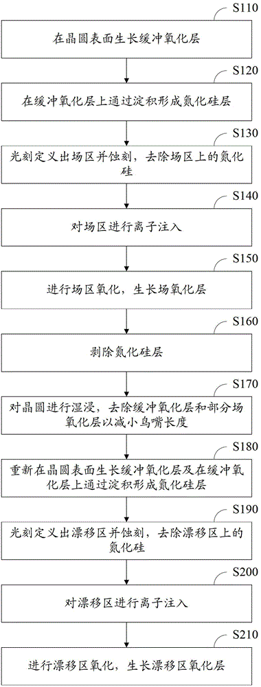
[0018] figure 1 It is a flowchart of a method for manufacturing a semiconductor device with a discrete field oxygen structure in an embodiment, including the following steps:

[0019] S110 , growing a buffer oxide layer (PAD oxide layer) on the surface of the wafer.

[0020] A buffer oxide layer can be grown on the surface of the silicon substrate by a thermal oxidation process. The buffer oxide layer can relieve the stress between the silicon and the subsequently deposited silicon nitride layer. The thicker the buffer oxide layer, the smaller the stress between silicon and silicon nitride, but the greater the effect on the shape and size of the active area. In this embodiment, the thickness of the buffer oxide layer is In other embodim...


PUM

PropertyMeasurementUnit
Thicknessaaaaaaaaaa
Thicknessaaaaaaaaaa
Thicknessaaaaaaaaaa

Abstract

The invention discloses a manufacturing method of a semiconductor device of a discrete field oxide structure. The method comprises steps: a buffer oxide layer grows on the surface of a wafer; a silicon nitride layer is formed on the buffer oxide layer through deposition; a field region is defined through photoetching and etching is carried out, and silicon nitride in the field region is removed; ion implantation is carried out on the field region; a field oxide layer grows; the silicon nitride layer is removed; wet dip is carried out on the wafer, and the buffer oxide layer and partial field oxide layer are removed; the buffer oxide layer grows again on the surface of the wafer and the silicon nitride layer is formed on the newly-grown buffer oxide layer through deposition; a drift region is defined through photoetching and etching is carried out, and silicon nitride in the drift region is removed; ion implantation is carried out on the drift region; and a drift region oxide layer grows. According to the method, the silicon nitride layer is removed after growing of the field oxide layer is finished, the length of a field oxide beak can be optimized through adjusting the amount of wet dip and the problem that the field oxide beak is excessively long can be solved.

Description

technical field [0001] The invention relates to the manufacture of the isolation region between components of the semiconductor device, in particular to a manufacturing method of the semiconductor device with a discrete field oxygen structure. Background technique [0002] In the design of modern integrated circuits, high-voltage lateral diffusion drift region MOS transistors (LDMOS) devices are widely used. The withstand voltage of LDMOS is realized by the principle of reducing the surface electric field (RESURF) by using the drift region of the drain end of the MOS transistor. This drift region is formed by ion implantation followed by diffusion through high temperature thermal processes. The drift region structure usually includes a thermal oxide layer with a certain thickness. Polysilicon is placed on the thermal oxide layer to change the potential distribution on the upper surface of the drift region to completely deplete the drift region and achieve the ultimate withst...

Claims


Application Information

Patent Timeline
IPC IPC(8): H01L21/762H01L21/336
CPCH01L21/76202H01L21/02238H01L21/26513H01L21/31111H01L21/32H01L21/76213H01L29/0653H01L29/66681H01L21/0217H01L21/02233H01L21/265H01L21/30604H01L21/31116H01L29/1095H01L29/408
Inventor 许剑何敏章舒罗泽煌吴孝嘉
Owner CSMC TECH FAB2 CO LTD
Why Eureka
Try Eureka