Semiconductor device of novel package structure

A packaging structure and semiconductor technology, applied in radiation control devices and other directions, can solve the problems of delamination and affect the reliability of CIS products, and achieve the effects of good chemical properties, high reliability, and stress relief.

Active Publication Date: 2014-07-30
苏州科阳半导体有限公司
View PDF5 Cites 4 Cited by
  • Summary
  • Abstract
  • Description
  • Claims
  • Application Information

AI Technical Summary

Problems solved by technology

Due to the limitation of overflowing glue, the width of the cofferdam is relatively large, which directly affects the reliability of CIS products and is prone to delamination.

Method used


Image

  • Semiconductor device of novel package structure
  • Semiconductor device of novel package structure
  • Semiconductor device of novel package structure

Examples


Embodiment

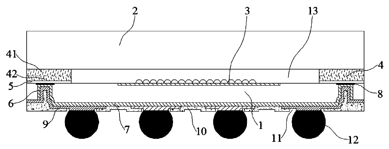
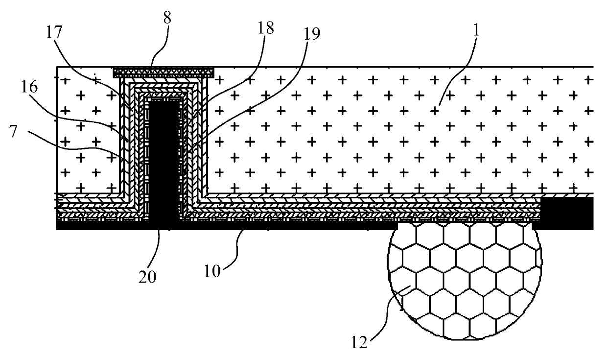
[0017] Embodiment: A semiconductor device with a new packaging structure, including an image sensing chip 1 and a transparent cover plate 2, the upper surface of the image sensing chip 1 has a photosensitive area 3, the edge of the transparent cover plate 2 and the image sensing chip There is a support dam 4 between the edges of the upper surface of 1 to form a cavity 13 between the transparent cover 2 and the image sensing chip 1, and the support dam 4 and the image sensing chip 1 are bonded by a glue layer 5 There are several blind holes 6 distributed around the edge area around the lower surface of the image sensor chip 1, the lower surface of the image sensor chip 1 and the side surfaces of the blind holes 6 have a passivation layer 7, and the bottom of the blind hole 6 has an image sensor The pin pad 8 of the chip 1, the surface of the passivation layer 7 opposite to the image sensor chip 1 and the blind hole 6 have a metal conductive pattern layer 9 electrically connected...


PUM


Abstract

The invention discloses a semiconductor device of a novel package structure. The semiconductor device comprises an image sensing chip and a transparent cover plate. A metal conductive pattern layer which is electrically connected with a pin bonding pad is arranged in a blind hole and on the surface, opposite to the image sensing chip, of a passivating layer. A supporting cofferdam is composed of a first supporting cofferdam layer and a second supporting cofferdam layer which are overlapped up and down. The first supporting cofferdam layer is in contact with the transparent cover plate. The second supporting cofferdam layer is in contact with the image sensing chip. A plurality of V-shaped continuous notches are formed in the inner side face of the second supporting cofferdam layer. Arc notches are formed in the four corners of the second supporting cofferdam layer respectively. The metal conductive pattern layer is formed by sequentially overlapping a titanium layer, a copper layer, a nickel layer and a palladium layer. The titanium layer and the passivating layer are in contact. The semiconductor device relieves stress, is exposed in the environment, and can not be easily oxidized and corroded, stress deformation of metal on the two sides of the blind hole under the cold and hot environments is effectively buffered, the response time of the semiconductor device is shortened, and the requirement that the metal layer continuously covers the inner wall of the deep hole with a high aspect ratio is met.

Description

technical field [0001] The invention relates to a semiconductor device with a novel packaging structure, belonging to the technical field of semiconductor packaging. Background technique [0002] Semiconductor devices refer to silicon wafers used in the production of silicon semiconductor integrated circuits. Because of their circular shape, they are called wafers; they can be processed into various circuit element structures on silicon wafers, and become ICs with specific electrical functions. product. The existing wafer-level chip packaging structure mainly has the following technical problems: [0003] (1) The existing metal yields filled in the blind holes on the wafer have certain limitations, high stress, low reliability level, and are easily oxidized and corroded in the exposed environment, resulting in product failure and stable chemical properties Poor, and with the development of wafer-level packaging through-hole silicon interconnection technology in the directi...

Claims


Application Information

Patent Timeline
Patent Type & Authority Applications(China)
IPC IPC(8): H01L27/146
Inventor 赖芳奇吕军张志良陈胜
Owner 苏州科阳半导体有限公司
Why Eureka
Try Eureka