Transistor based on multi-top-gate structure

A transistor and top-gate technology, applied in the field of microelectronics, can solve problems such as difficulty in guaranteeing the yield of logic circuits and complicated manufacturing process, and achieve the effects of volume reduction, production cost reduction, and number reduction

Active Publication Date: 2014-07-30
NINGBO INST OF MATERIALS TECH & ENG CHINESE ACADEMY OF SCI
View PDF5 Cites 4 Cited by
  • Summary
  • Abstract
  • Description
  • Claims
  • Application Information

AI Technical Summary

Problems solved by technology

[0006] Logic circuits in the traditional sense, in order to realize different logic gate operations, need to use different types, different types, and different numbers of transistors, thereby putting forward higher requirements for the process of making logic circuits in large areas, including using different masks. Stencils, different processes, different materials and different designs, so the manufacturing process is more complicated, and the yield of logic circuits is difficult to guarantee

Method used


Image

  • Transistor based on multi-top-gate structure
  • Transistor based on multi-top-gate structure
  • Transistor based on multi-top-gate structure

Examples


Embodiment 1

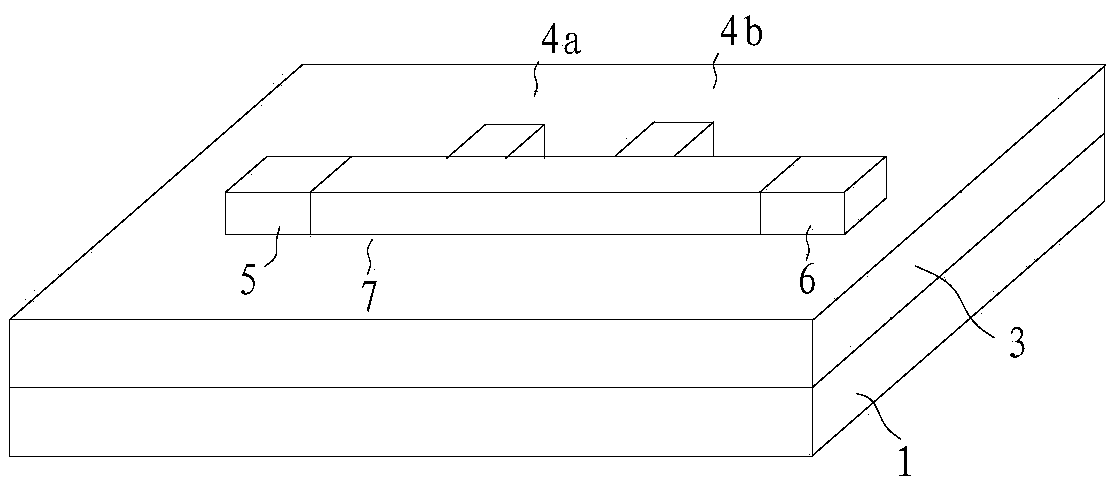
[0088] Such as figure 1 As shown, a transistor based on a multi-top gate structure includes a substrate 1 and a dielectric layer 3 on the substrate 1. A source region 5 and a drain region 6 are arranged on the dielectric layer 3, and are connected to the source region 5 and the drain region. In the channel region 7 between 6, two top gates are respectively the first top gate 4a and the second top gate 4b, both of which are connected to the channel region 7. The first top gate 4a is used as an output pole, and the second top gate 4b is used as an input pole.

[0089] Such as figure 2 As shown, the first top gate 4a and the second top gate 4b are connected to the channel region 7, and the channel region 7 can be extended to form a ledge, and the first top gate 4a and the second top gate 4b are connected to the channel through the ledge. District 7 is connected.

[0090] The substrate 1 is made of glass with a single surface as a conductive layer, the conductive layer is made...

Embodiment 2

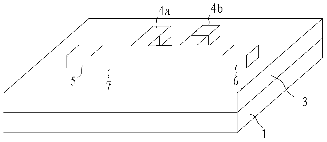
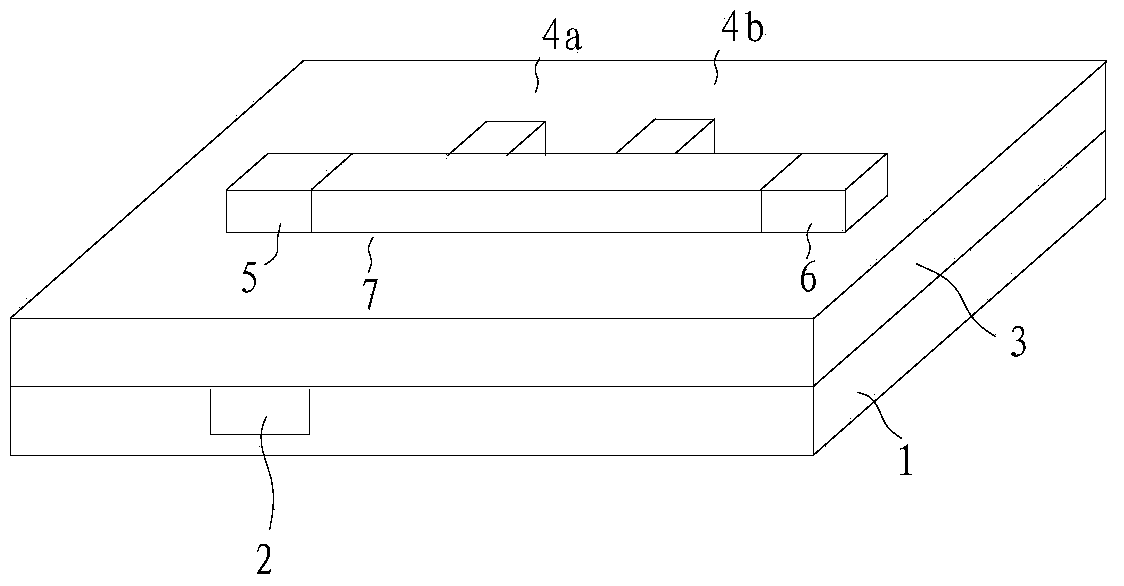
[0098] Such as image 3 As shown, a transistor based on a multi-top gate structure includes a substrate 1 and a dielectric layer 3 on the substrate 1. A source region 5 and a drain region 6 are arranged on the dielectric layer 3, and are connected to the source region 5 and the drain region. The channel region 7 between 6, the two top gates, and the bottom gate 2 coupled with the two top gates. The two top gates are respectively a first top gate 4 a and a second top gate 4 b, both of which are connected to the channel region 7 . The bottom gate 2 is located between the substrate 1 and the dielectric layer 3, the bottom gate 2 is distributed in a local area on the substrate 1, and the substrate 1 is provided with an accommodation groove corresponding to the position of the bottom gate 2, and the area of ​​the bottom gate 2 can be controlled at least channel region 7. If there is no bottom gate, add a top gate outside the channel to replace the bottom gate to regulate the chan...

Embodiment 3

[0108] Such as Figure 4 The shown transistor based on the multi-top gate structure includes a substrate 1 and a dielectric layer 3 on the substrate 1. A source region 5 and a drain region 6 are arranged on the dielectric layer 3, and are connected between the source region 5 and the drain region 6. The channel region 7 between them, and the three top gates are the first top gate 4a, the second top gate 4b and the third top gate 4c respectively, wherein the first top gate 4a, the second top gate 4b and the first top gate The three top gates 4c are all connected to the channel region 7, and the substrate 1 also serves as the bottom gate.

[0109] The substrate 1 is made of glass with a single surface as a conductive layer, the conductive layer is made of indium tin oxide (ITO) and the dielectric layer 3 is bonded, the dielectric layer 3 is made of silicon dioxide, and the physical thickness of the dielectric layer 3 is 0.5 μm; the source region 5. The drain region 6, the first...


PUM


Abstract

The invention discloses a transistor based on a multi-top-gate structure. The transistor comprises a substrate and a dielectric layer located on the substrate. The dielectric layer is provided with a source region, a drain region and a channel region connected between the source region and the drain region. The channel region is connected with at least two top gates, one of the top gates serves as an output pole, and the rest of the top gates serve as input poles. The source region, the drain region and all the top gates are arranged on the lower surface of the dielectric layer in a co-plane mode. The transistor is provided with one or more input poles used for controlling current carriers of the channel region, the voltage of the input poles is changed and the output state of the transistor is controlled, so that one transistor is used for achieving multiple logic outputs, the number of transistors in a logic circuit can be reduced, and the manufacturing method of the logic circuit is simple. The co-plane design of the top gates and a channel is adopted, the size of the transistor is effectively reduced, the integration level of the logic circuit is easily improved, and manufacturing cost is reduced.

Description

technical field [0001] The invention belongs to the technical field of microelectronics, and in particular relates to a transistor based on a multi-top gate structure. Background technique [0002] A transistor is a solid-state semiconductor device that can be used for detection, rectification, amplification, switching, voltage regulation, signal modulation, and many other functions. As a variable switch, the transistor controls the outgoing current based on the input voltage, so the transistor can be used as a current switch. The difference from general mechanical switches is that the transistor is controlled by electrical signals, and the switching speed can be very fast. The switching speed in the laboratory can reach more than 100GHz. [0003] Transistors can be divided into two main categories: Bipolar Transistors (BJTs) and Field Effect Transistors (FETs). The transistor has three poles; the three poles of the bipolar transistor are the emitter, base and collector co...

Claims


Application Information

Patent Timeline
Patent Type & Authority Applications(China)
IPC IPC(8): H01L29/78H01L29/786H01L29/423
CPCH01L29/4232H01L29/7831
Inventor 戴明志
Owner NINGBO INST OF MATERIALS TECH & ENG CHINESE ACADEMY OF SCI
Why Eureka
Try Eureka