Thermoelectric material, method for producing same, and thermoelectric conversion module using same

A technology of thermoelectric materials and thermoelectric layers, which is applied in the manufacture/processing of thermoelectric devices, materials for the junction leads of thermoelectric devices, thermoelectric devices that only use the Peltier or Seebeck effect, etc., can solve the problems of thermal conductivity reduction and achieve increased Effect of power factor and conductivity improvement

Active Publication Date: 2014-07-30
JAPAN SCI & TECH CORP
View PDF5 Cites 4 Cited by
  • Summary
  • Abstract
  • Description
  • Claims
  • Application Information

AI Technical Summary

Problems solved by technology

[0007] In addition, it has been reported that the use of materials with a nanodot structure leads to a decrease in thermal conductivity (Non-Patent Document 9)

Method used


Image

  • Thermoelectric material, method for producing same, and thermoelectric conversion module using same
  • Thermoelectric material, method for producing same, and thermoelectric conversion module using same
  • Thermoelectric material, method for producing same, and thermoelectric conversion module using same

Examples


no. 1 approach

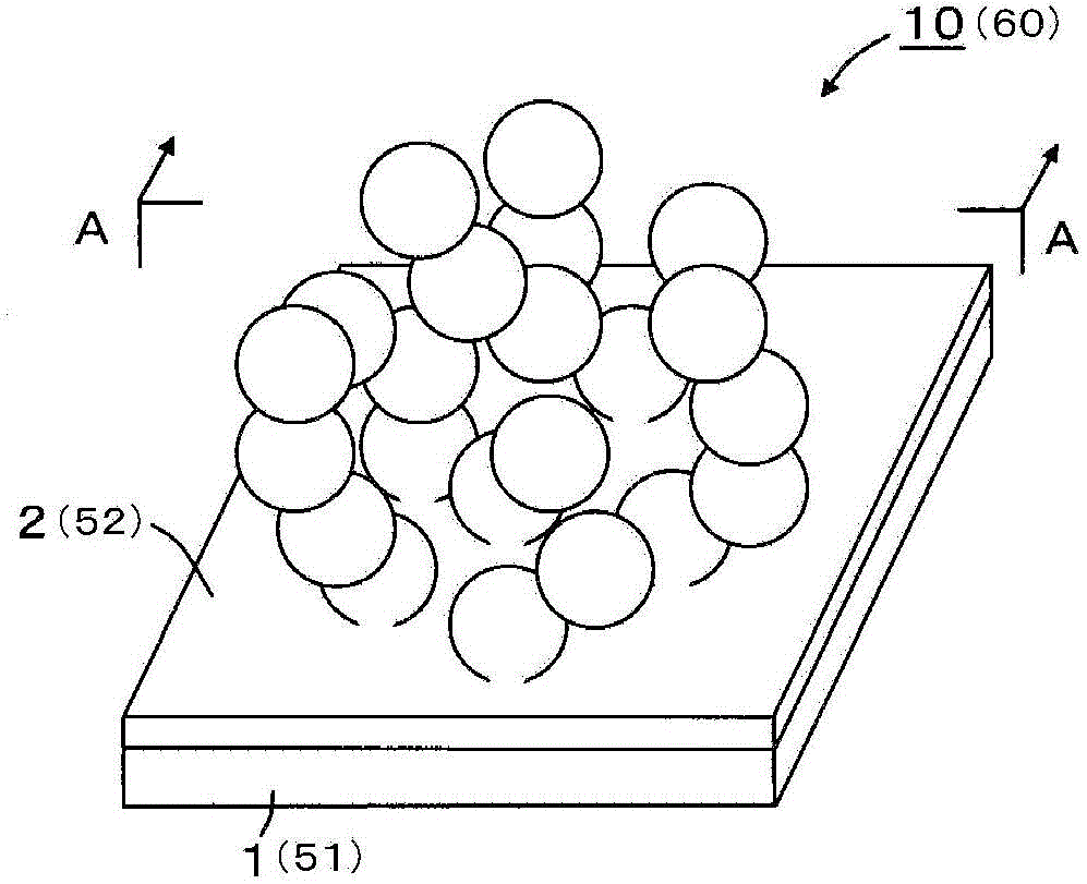
[0066] will refer to figure 1 and 2 A thermoelectric material 10 according to a first embodiment of the present invention is described.

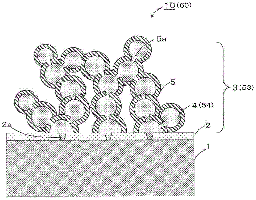
[0067] as in figure 1 and 2 As shown in , the thermoelectric material 10 includes a silicon substrate 1 , a silicon oxide film 2 formed on the silicon substrate 1 , and a thermoelectric layer 3 disposed on the silicon oxide film 2 . As the silicon substrate 1, a single crystal silicon substrate is preferably used. The silicon oxide film 2 is preferably an ultra-thin oxide film as thick as about a single layer or double layers of Si. The thermoelectric layer 3 has a configuration in which a plurality of semiconductor nanodots 4 each surrounded by a barrier layer (hereinafter, referred to as a barrier layer) 5 are stacked so as to form a particle-filled structure.

[0068] Nanodots herein refer to nanocrystals having nanoscale dimensions having a substantially spherical or substantially elliptical shape. It is to be noted that the nanodo...

no. 2 approach

[0104] Reference will be made to describe the first embodiment figure 1 etc. describe the thermoelectric material 60 according to the second embodiment of the present invention.

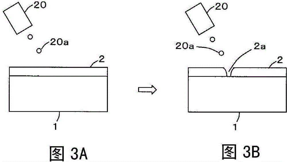
[0105] In the growing step S4 of the method for manufacturing a thermoelectric material according to the first embodiment, irradiation is performed with a molecular beam of the material (eg, Si, Ge, SiGe, or silicide of nanodots 4) (see Figures 4A to 4C ). Meanwhile, in the growing step S4 according to this embodiment, irradiation is performed with a molecular beam of a dopant (ie, a donor atom or an acceptor atom other than the molecular beam of the material of the nanodots 54 ). Thus, the nanodots 54 of the thermoelectric layer 53 are doped, and the thermoelectric material 60 functions as a p-type semiconductor or an n-type semiconductor. Except for the above, the configuration of the thermoelectric material 60 and the steps of the method of manufacturing the thermoelectric material 60 are the s...


PUM


Abstract

This thermoelectric material is provided with a semiconductor substrate, a semiconductor oxide film that is formed on the substrate, and a thermoelectric layer that is arranged on the oxide film. The semiconductor oxide film is provided with a first nano-opening, and the thermoelectric layer is in the form of a plurality of semiconductor nano-dots piled up on the first nano-opening so as to have a particle packed structure. At least some of the plurality of semiconductor nano-dots have second nano-openings formed in the surfaces thereof, and are connected with each other through the second nano-openings, with the crystal orientations thereof being aligned with each other. This thermoelectric material can be produced through: a step wherein a semiconductor substrate is oxidized, thereby forming a semiconductor oxide film thereon; a step wherein a first nano-opening is formed in the oxide film; and a step wherein a plurality of semiconductor nano-dots are piled up on the first nano-opening by epitaxial growth. A thermoelectric material having excellent thermoelectric conversion performance can be achieved by this configuration.

Description

technical field [0001] The present invention relates to thermoelectric materials using semiconductor nanodots (nanodots), and more particularly to thermoelectric materials including nanodots made of silicon, germanium, or silicon-based semiconductors, and thermoelectric conversion modules using the thermoelectric materials, and manufacturing The method of the thermoelectric material. Background technique [0002] Recently, in order to reduce environmental load, thermoelectric conversion technology for efficient use of energy has attracted attention. Accordingly, high-performance thermoelectric materials using rare earth metals such as BiTe, PbTe, or SiGe have been conventionally developed as thermoelectric materials for use in thermoelectric conversion technologies using the Seebeck effect. However, in this case, since rare earth metals are used, there are problems of environmental load and risk in terms of resources. [0003] When evaluating thermoelectric conversion perf...

Claims


Application Information

Patent Timeline
Patent Type & Authority Applications(China)
IPC IPC(8): H01L35/32H01L35/14H01L35/34
CPCH10N10/857H10N10/855H10N10/00H10N10/01H10N10/17H10N10/85H10N10/851
Inventor 中村芳明五十川雅之上田智广吉川纯酒井朗细野秀雄
Owner JAPAN SCI & TECH CORP
Why Eureka
Try Eureka