Method for optimizing shape of ion implantation region

A technology of ion implantation and area, applied in electrical components, semiconductor/solid-state device manufacturing, circuits, etc., can solve the problems affecting the quality of ion implantation and the morphology of ion implantation area, corrosion damage of substrate surface, reducing device quality and yield, etc.

Active Publication Date: 2014-08-06
SHANGHAI HUALI MICROELECTRONICS CORP
View PDF8 Cites 5 Cited by
  • Summary
  • Abstract
  • Description
  • Claims
  • Application Information

AI Technical Summary

Problems solved by technology

Patent No. CN100561664C discloses a method for removing residual polymers after etching, which uses plasma dry etching to remove residual polymers. However, in the removal process, it is difficult to accurately control the etching depth, which is easy to cause over-etching , it will aggravate the damage to the substrate surface and the above-mentioned oxide layer. The above-mentioned oxide layer is a buffer layer for subsequent ion implantation, which is used to control the depth of ion implantation and alleviate the excessive energy of ion implantation so as to avoid ion implantation. Tunneling effect defects, if the oxide layer is damaged, will reduce its effect as a buffer layer, which will still affect the quality of the subsequent ion implantation process and the morphology of the ion implantation area, resulting in a decrease in device performance. It is difficult to remove the insoluble residual oxide by bulk dry etching
[0011] Patent No. CN100392821C discloses a method for removing residual polymers from etching, which uses a combination of plasma bombardment and wet etching to remove residual polymers, which undoubtedly increases the cost and also increases the burden on the The damage caused by the surface of the substrate and the above-mentioned oxide layer affects the quality of the subsequent ion implantation process and the morphology of the ion implantation area, reducing the quality and yield of the device
[0012] The patent No. CN1840624A discloses a polymer remover, which contains a large amount of organic acid compounds such as fluoride ion source, water, trihaloacetic acid, organic polycarboxylic acid compound, organic hydroxycarboxylic acid compound, amino acid, etc. Organic solvents are not only costly, but the pH value must be strictly controlled, otherwise it is easy to cause corrosion damage to the substrate surface and the above-mentioned oxide layer, which will still affect the quality of ion implantation and the morphology of the ion implantation area, reducing device quality and yield
[0013] Patent No. CN100468618C discloses a semiconductor device manufacturing method for removing residual polymer after etching, which uses a method of combining cleaning and heat treatment of the etched substrate to remove etching by-products. The cleaning method is still a conventional wet cleaning process. Although the heat treatment process can remove insoluble polymers, the high-temperature process during the heat treatment process will greatly increase the damage to the substrate surface and the above-mentioned oxide layer, thereby affecting the subsequent ions. The quality of the implantation process and the morphology of the ion implantation area further affect the quality and yield of the device

Method used


Image

  • Method for optimizing shape of ion implantation region
  • Method for optimizing shape of ion implantation region
  • Method for optimizing shape of ion implantation region

Examples


Embodiment 1

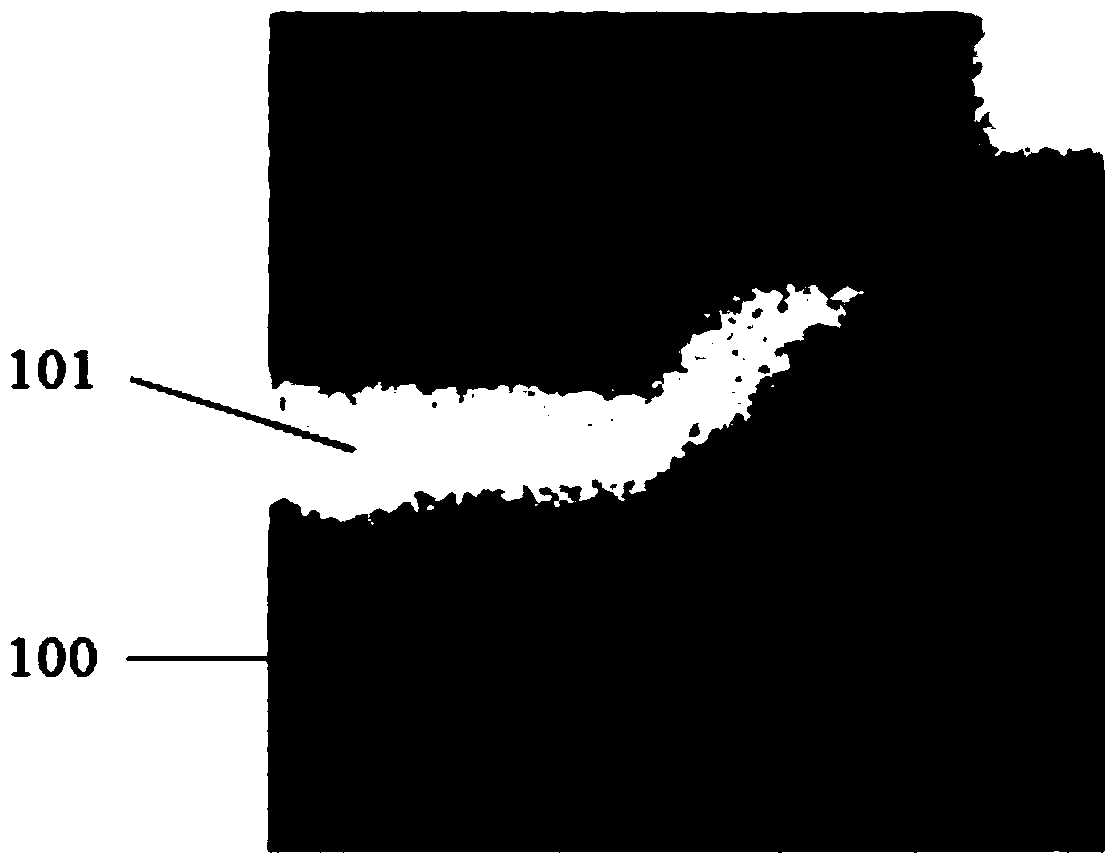
[0042] The following will be combined with Figure 3-9 The method for optimizing the morphology of the ion implantation region of the present invention will be further described in detail with specific embodiments. in, image 3 It is a schematic flow chart of the method for optimizing the morphology of the ion implantation region of the present invention, Figure 4-9It is a schematic diagram of the structure formed by each preparation step of the method for optimizing the morphology of the ion implantation region according to the first embodiment of the present invention. It should be noted that the drawings are all in a very simplified form, using imprecise scales, and are only used to facilitate and clearly achieve the purpose of assisting in describing the present embodiment.

[0043] see image 3 , the method for optimizing the morphology of the ion implantation region of the present invention, comprising:

[0044] Step S01: See Figure 4 , providing a semiconductor d...

Embodiment 2

[0069] The method for optimizing the morphology of the ion implantation region in the second embodiment can be the same as that in the first embodiment; the difference with respect to the first embodiment is that the etching by-products in the second embodiment remain on the surface of the original oxide layer at the top of the gate , or there are residues on both the surface of the original oxide layer on the top of the gate and the surface of the original oxide layer on the substrate of the semiconductor device. The method for removing the residual oxide is the same as the first embodiment, no matter where the etching by-products remain on the original oxide layer, the removal process is still to remove the original oxide layer on the top of the gate and the surface of the semiconductor device substrate. Then, a new oxide layer is grown on the entire semiconductor device substrate, and the new oxide layer covers the tops of the gate and sidewalls, the sidewalls of the sidewal...


PUM


Abstract

The invention provides a method for optimizing the shape of an ion implantation region. The method includes the steps that a semiconductor device substrate with a grid is provided; original oxidization layers and nitration layers are sequentially deposited on the surface of the semiconductor device substrate, the top of the grid and the side walls of the grid; the nitration layer on the top of the grid and the nitration layer on the surface of the semiconductor device substrate are subjected to over etching so that side walls can be formed; etching by-products are formed on the original oxidization layers; the semiconductor device substrate is cleaned with a wet method, and the etched by-products change into residual oxide; the surfaces of the original oxidization layers with the residual oxide or the whole original oxidization layers with the residual oxide are removed, then, an oxidization layer is grown on the semiconductor device substrate so that a new oxidization layer can be formed, and the new oxidization layer can replace the original oxidization layer to serve as a buffer layer for subsequent ion implantation. According to the method, while the residual oxide can be effectively removed in a controllable mode, the ion implantation quality is further improved, the shape of a subsequent ion implantation region is optimized, the quality of devices is improved, and the yield of the devices is increased.

Description

technical field [0001] The invention relates to the technical field of semiconductors, in particular to a method for optimizing the morphology of ion implantation regions. Background technique [0002] With the development of integrated circuit technology and the scaling down of critical dimensions, the process window of various processes is getting smaller and smaller. The ion implantation process has an important impact on the performance and yield of the device, such as the depth of ion implantation, dose and even the size of the ion implantation area. shape and so on. [0003] Typically, ion implantation methods include: [0004] Provide a semiconductor device substrate with an oxide layer on its surface; [0005] Etching and forming a gate structure in the substrate of the semiconductor device; [0006] Wet cleaning of semiconductor device substrates; [0007] An ion implantation process is performed into the semiconductor device substrate. [0008] Here, the ion i...

Claims


Application Information

Patent Timeline
Patent Type & Authority Applications(China)
IPC IPC(8): H01L21/265
CPCH01L21/02057H01L21/02096H01L21/26506
Inventor 范荣伟陈宏璘龙吟顾晓芳
Owner SHANGHAI HUALI MICROELECTRONICS CORP
Why Eureka
Try Eureka