Semiconductor device manufacturing method

A device manufacturing method and semiconductor technology, applied in semiconductor/solid-state device manufacturing, semiconductor devices, transistors, etc., can solve problems such as rough edges, inability to integrate large-scale, and inability to narrow the width of nano-bands, and achieve high integration, suitable for For large-scale integration, low edge roughness

Active Publication Date: 2018-02-13
INST OF MICROELECTRONICS CHINESE ACAD OF SCI
View PDF4 Cites 0 Cited by
  • Summary
  • Abstract
  • Description
  • Claims
  • Application Information

AI Technical Summary

Problems solved by technology

[0007] In view of the existing problems in the preparation of graphene nanoribbons, such as the width of the nanoribbons cannot be narrowed, the edges are rough, and large-scale integration cannot be achieved. craft

Method used


Image

  • Semiconductor device manufacturing method
  • Semiconductor device manufacturing method
  • Semiconductor device manufacturing method

Examples


Embodiment Construction

[0025] Hereinafter, the present invention is described by means of specific embodiments shown in the drawings. It should be understood, however, that these descriptions are exemplary only and are not intended to limit the scope of the present invention. Also, in the following description, descriptions of well-known structures and techniques are omitted to avoid unnecessarily obscuring the concept of the present invention.

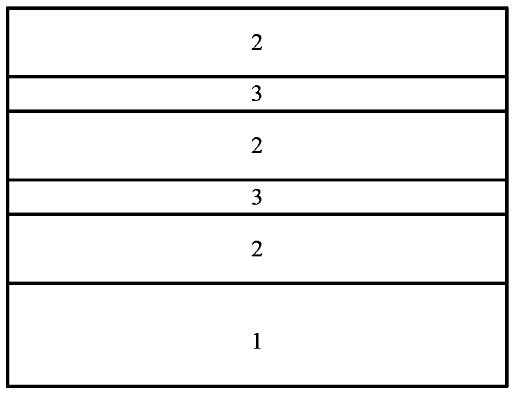
[0026] The invention provides a method for manufacturing a semiconductor device, which uses a lamination method to self-limit the growth of graphene nanobelts. For the manufacturing process, see the appended Figure 1-7 .

[0027] First, see attached figure 1 , providing a substrate 1 . The substrate 1 in the present invention can be a substrate processed by at least one process, and its material can be semiconductor materials such as silicon, gallium nitride, and silicon germanium, or other insulating media such as glass, and the selection of specific m...


PUM

PropertyMeasurementUnit
thicknessaaaaaaaaaa
thicknessaaaaaaaaaa

Abstract

The invention provides a method for manufacturing a graphene device. The graphene nanobelt device is grown in a self-limited mode on the base of the layer stacking method. According to the method for manufacturing the graphene device, through the stacked layer structure of a plurality of dielectric layers and metal layers, a graphene nanobelt is grown on the side face of each metal layer in situ in a self-limited mode; due to the fact that the number of the metal layers and the thickness of each metal layer are set, the high-precision graphene nanobelts with the widths being below 5 nm can be obtained, and the widths and uniformity of the graphene nanobelts can be highly controlled. The method for manufacturing the graphene device has the advantages of being high in throughput and suitable for large-scale integration. Meanwhile, the graphene nanobelts manufactured with the method are low in edge roughness and capable of being used for manufacturing the three-dimensional graphene device, so that the high integration level is achieved.

Description

technical field [0001] The invention relates to the field of semiconductor device manufacturing methods, in particular to a semiconductor device manufacturing method using a lamination method for self-limited growth of graphene nanobelts. Background technique [0002] Since the first transistor was invented, integrated circuits have been advancing at breakneck speed, fueled by a series of innovative efforts. Today, the feature size of silicon-based integrated circuits has dropped to 22nm, and a lot of progress has been made in 16nm and 14nm node technologies. However, how to continue to promote the development of integrated circuits in a high-speed development mode has become a problem that has to be considered. In recent years, new materials, new processes, and new devices have emerged continuously, especially new materials have received more widespread attention. What kind of materials can occupy new heights in the post-silicon era has become a research hotspot for scient...

Claims


Application Information

Patent Timeline
Patent Type & Authority Patents(China)
IPC IPC(8): H01L21/336
CPCB82Y10/00H01L21/02527H01L21/02603H01L29/1606H01L29/66045
Inventor 贾昆鹏朱慧珑
Owner INST OF MICROELECTRONICS CHINESE ACAD OF SCI
Why Eureka
Try Eureka